Light-emitting device
a technology of light-emitting devices and structures, which is applied in the direction of solid-state devices, semiconductor devices, thermoelectric devices, etc., can solve the problems of light-emission elements included in them that undergo degradation, and achieve the effect of reducing the amount of heat and effectively discharging hea
- Summary
- Abstract
- Description
- Claims
- Application Information
AI Technical Summary
Benefits of technology
Problems solved by technology
Method used
Image
Examples
embodiment 1
1. Overall Structure
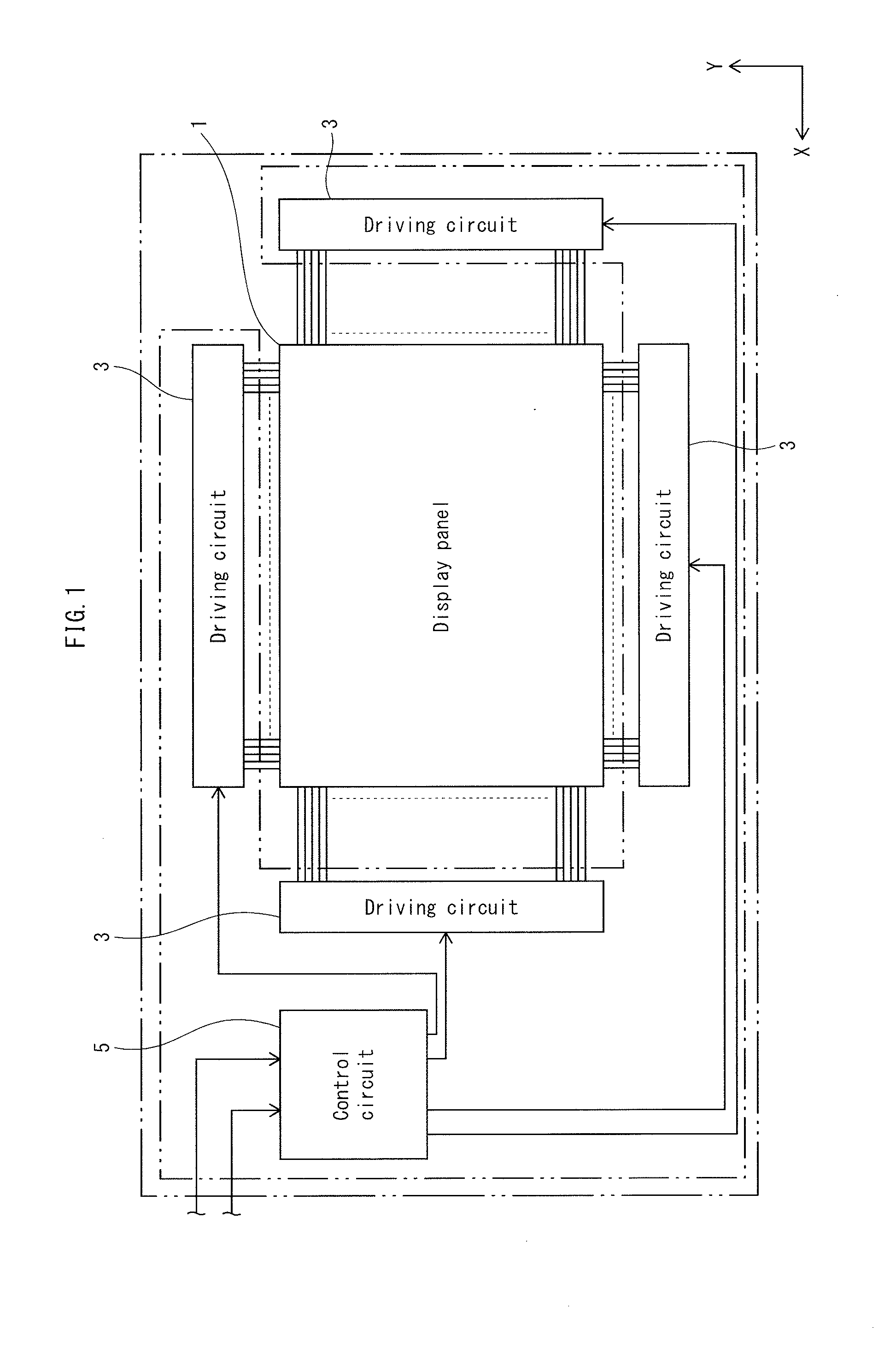
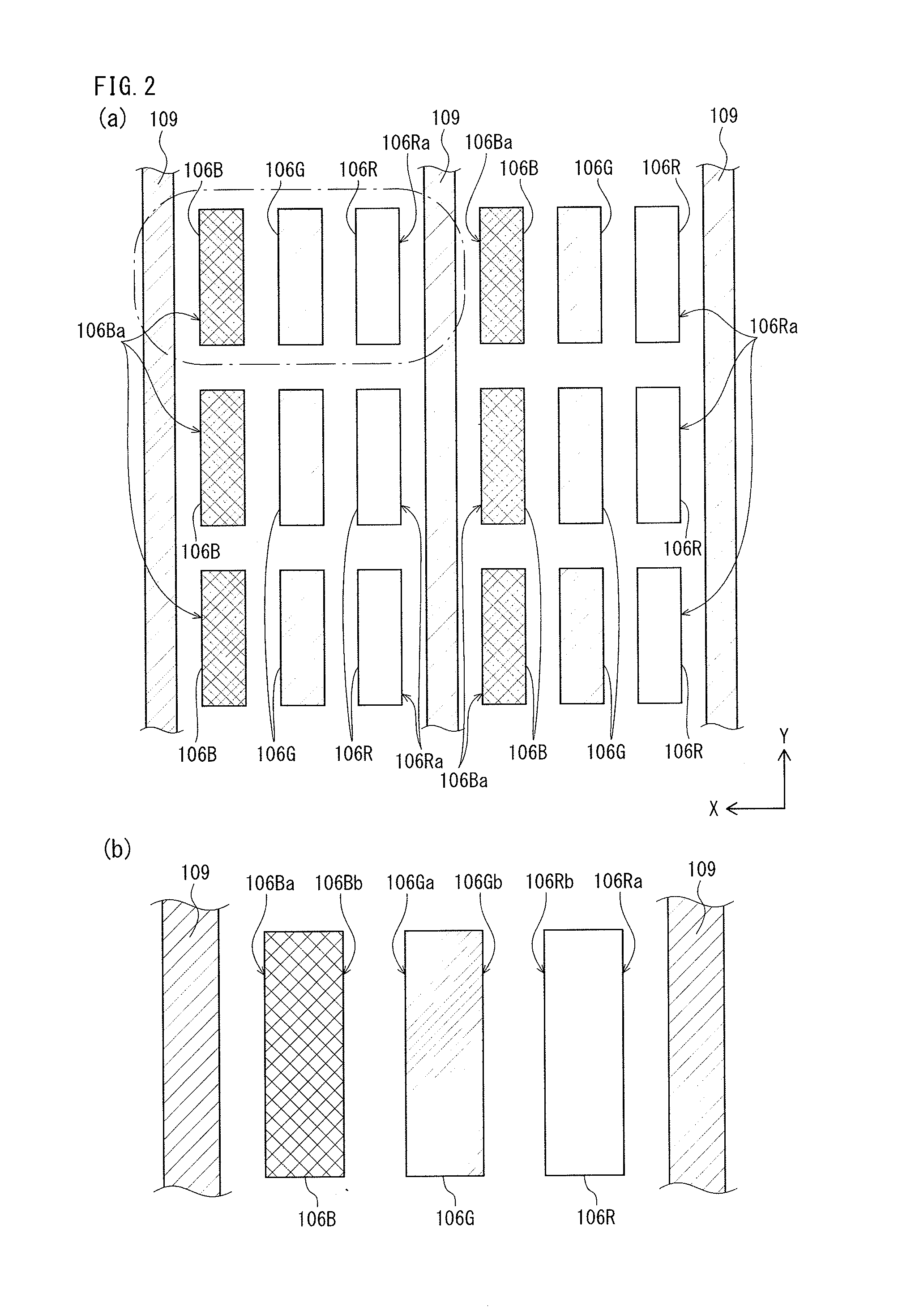
[0033]In the following, description is provided on one embodiment of the present invention, with reference to the accompanying drawings. FIG. 1 is a schematic block diagram illustrating an overall structure of a light-emission device including an organic EL display panel 1 pertaining to embodiment 1 of the present invention. Here, the organic EL display panel 1 is a top-emission type organic EL display panel. That is, light emitted by a light-emission layer disposed above a glass substrate is guided out from a side of the organic EL display panel 1 opposite the glass substrate with respect to the light-emission layer. Further, the organic EL display panel 1 does not include an electron injection layer, a hole injection layer, or a color filter. As such, in the organic EL display panel 1, a light-emission layer corresponds to a light-emission unit.
[0034]As illustrated in FIG. 1, driving circuits 3 are connected to the organic EL display panel 1. A control circuit ...
embodiment 2
[0052]In the following, description is provided on embodiment 2 of the present invention, differing from embodiment 1 in terms of the shape of the wiring layer. As such, note that description on structures similar to embodiment 1 is omitted hereafter.
[0053]FIG. 6 is a plan view illustrating a layout of light-emission layers and a wiring layer in an organic EL display panel pertaining to embodiment 2.
[0054]As illustrated in FIG. 6, a wiring layer 209 in the organic EL display panel pertaining to embodiment 2 includes line portions 209a and extending portions 209b. The line portions 209a are each formed to have the shape of a line. Each of the extending portions 209b extends from one of the line portions 209a and extends to oppose a short side of the B light-emission layer 106B.
[0055]In the above-described structure of the organic EL display panel pertaining to embodiment 2, the B light-emission layers 106B, which generates the greatest amount of heat among the light-emission layers 1...
embodiment 3
[0056]In the following, description is provided on another embodiment of the present invention, differing from embodiment 2 in terms of the shape of the wiring layer. As such, note that description on structures similar to embodiments 1 and 2 are omitted hereafter.
[0057]FIG. 7 is a plan view illustrating a layout of light-emission layers and a wiring layer in an organic EL display panel pertaining to embodiment 3.
[0058]As illustrated in FIG. 7, a wiring layer 309 in the organic EL display panel pertaining to embodiment 3 includes line portions 309a and extending portions 309b. The line portions 309a are each formed to have the shape of a line. Each of the extending portions 309b extend from one of the line portions 309a to an adjacent one of the line portions 309a. Due to this, the wiring layer 309, when seen as a whole, has the shape of a matrix.
[0059]In the above-described structure of the organic EL display panel pertaining to embodiment 3, the G light-emission layer 106G has a f...
PUM
 Abstract
Description
Claims
Application Information
 - R&D
- Intellectual Property
- Life Sciences
- Materials
- Tech Scout
- Unparalleled Data Quality
- Higher Quality Content
- 60% Fewer Hallucinations
Browse by: Latest US Patents, China's latest patents, Technical Efficacy Thesaurus, Application Domain, Technology Topic, Popular Technical Reports.
© 2025 PatSnap. All rights reserved.Legal|Privacy policy|Modern Slavery Act Transparency Statement|Sitemap|About US| Contact US: help@patsnap.com


