Low-Pin-Count Non-Volatile Memory Interface

a non-volatile memory and pin-count technology, applied in static storage, digital storage, instruments, etc., can solve the problems of reducing the size the number of external interface pins becomes a limitation of the otp memory size, and the cost of otp memory to be integrated into the integrated circuit is relatively high, so as to reduce the area and footprint, the effect of reducing the area and footprin

Active Publication Date: 2015-03-19
ATTOPSEMI TECH CO LTD
View PDF1 Cites 39 Cited by
  • Summary
  • Abstract
  • Description
  • Claims
  • Application Information

AI Technical Summary

Benefits of technology

[0009]The invention relates to a low-pin-count non-volatile memory (NVM) having reduced area and footprint. In one embodiment, the low-pin-count non-volatile memory can use an interface that makes use of only one pin external to an integrated circuit. This interface not only can use only one external pin but also can share several internal pins with the rest of integrated circuit to thereby reduce area and footprint. Moreover, if desired, the one external pin can be further multiplexed with the other pins so that no additional pins are needed. In one embodiment the interface can pertain to a low-pin-count OTP interface for an OTP memory so that the OTP memory can be easily integrated into an integrated circuit.

Problems solved by technology

Since there are several I / O pins, the footprint of an OTP memory to be integrated into an integrated circuit the cost is relatively high.
In an OTP, the program time is several orders of magnitude higher than the read access and much lower than either the program or erase time of EEPROM, for example 1 us versus 50 ns for read and 1 us versus 4 ms for program / erase, such that I2C interface for OTP is not desirable because of high timing overhead.
As OTP memory sizes continue to be reduced, the number of external interface pins becomes a limitation to the OTP memory size.
The current serial interfaces have about 2-4 pins and are not able to effectively accommodate read and program speed discrepancies.

Method used


Image

  • Low-Pin-Count Non-Volatile Memory Interface
  • Low-Pin-Count Non-Volatile Memory Interface
  • Low-Pin-Count Non-Volatile Memory Interface

Examples


Embodiment Construction

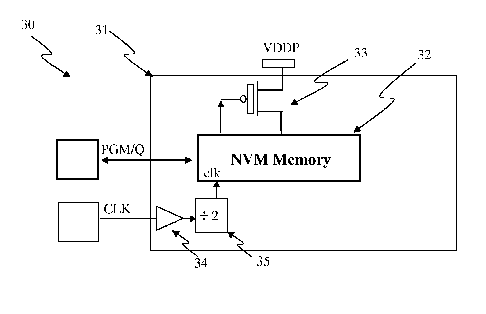
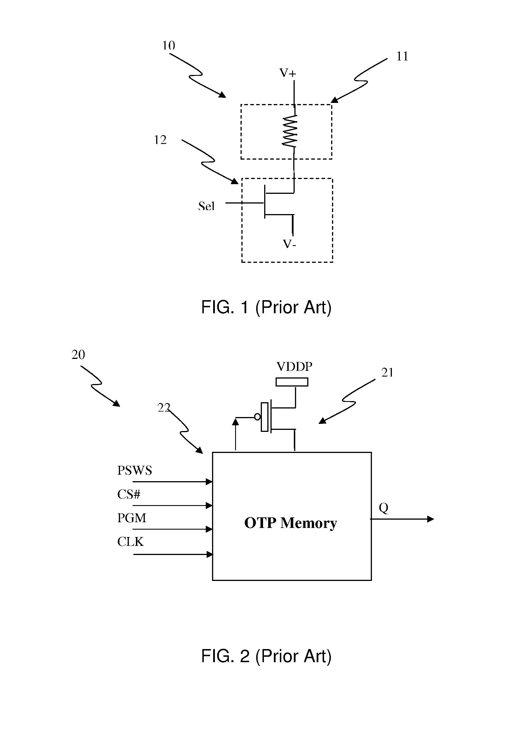
[0036]The invention relates to a low-pin-count non-volatile memory (NVM) having reduced area and footprint. In one embodiment, the low-pin-count non-volatile memory can use an interface that makes use of only one pin external to an integrated circuit. This interface not only can use only one external pin but also can share several internal pins with the rest of integrated circuit to thereby reduce area and footprint. Moreover, if desired, the one external pin can be further multiplexed with the other pins so that no additional pins are needed. In one embodiment the interface can pertain to a low-pin-count OTP interface for an OTP memory so that the OTP memory can be easily integrated into an integrated circuit.

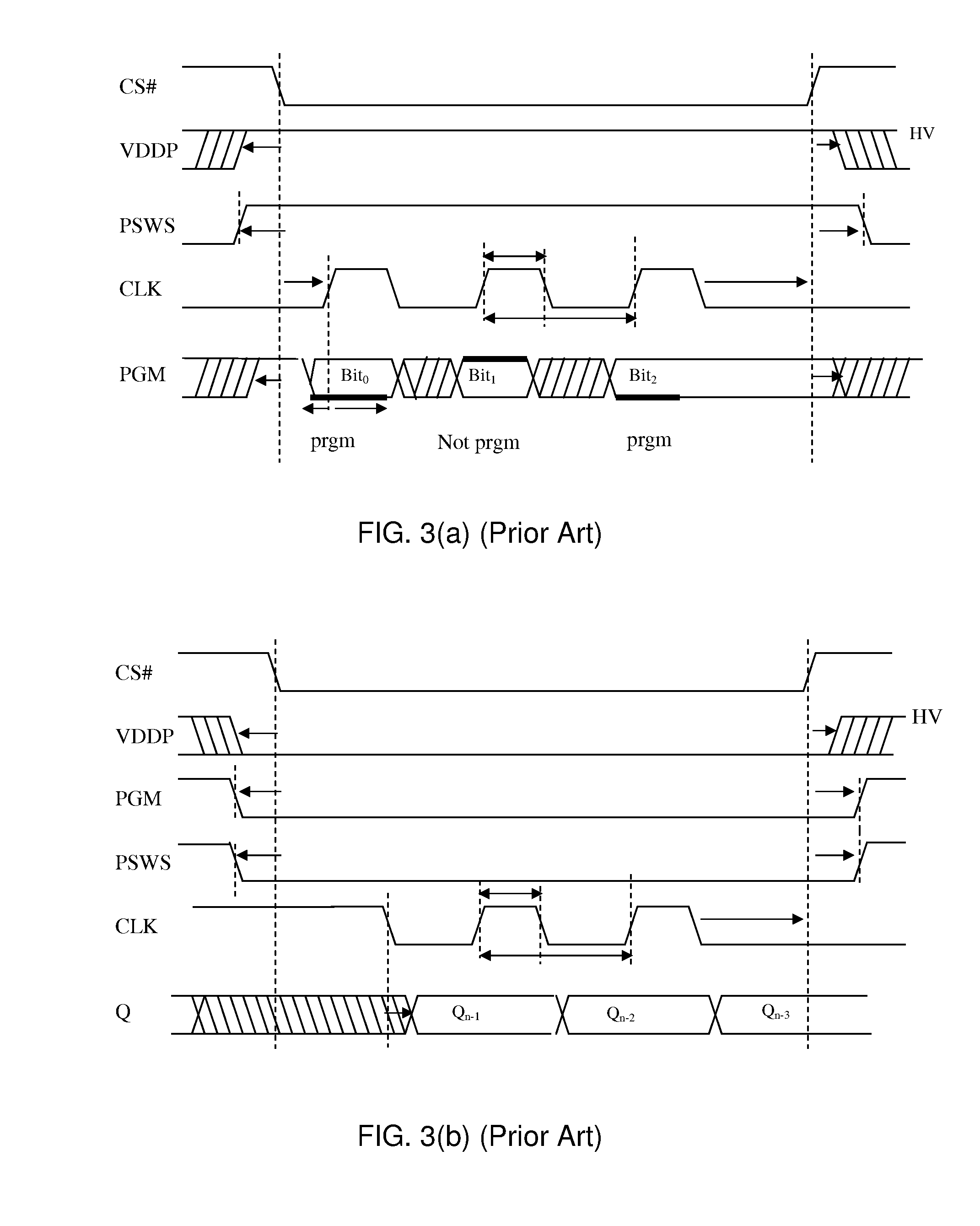
[0037]Simply employing a serial interface is not sufficient for an OTP memory because an OTP memory requires high voltage programming control and has a much longer program time than read time. Also, getting into a program mode at a specific address should be immune to noises a...


PUM


Abstract

A low-pin-count non-volatile (NVM) memory to be provided in an integrated circuit. The low-pin-count non-volatile (NVM) memory can use only one external control signal and one internal clock signal to generate start, stop, device ID, read / program / erase pattern, starting address, and actual read / program / erase cycles. When programming or erasing begins, toggling of the control signal increments / decrements a program or erase address and a pulse width of the control signal determines the actual program or erase time. A data out of the low-pin-count non-volatile (NVM) memory can be multiplexed with the control signal. In some applications where only the integrated circuit can read the data, a second control signal internal to the integrated circuit generates start, stop, device ID, read pattern, starting address, and actual read cycles, while the first control signal external to the integrated circuit can do the same for the program or erase path. Since the clock signal can be derived and shared from the system clock of the integrated circuit, the NVM memory need only have one external control pin for I / O transactions to realize a low-pin-count interface.

Description

CROSS-REFERENCE TO RELATED APPLICATION[0001]This application is a continuation of U.S. patent application Ser. No. 13 / 288,843, filed on Nov. 3, 2011 and entitled “Low-In-Count Non-Volatile Memory Interface,” which is hereby incorporated herein by reference, which in turn claims priority benefit of: U.S. Provisional Patent Application No. 61 / 409,539, filed on Nov. 3, 2010 and entitled “Circuit and System of A Low Pin Count One-Time-Programmable Memory,” which is hereby incorporated herein by reference.BACKGROUND OF THE INVENTION[0002]Non-volatile memory (NVM) is able to retain data when the power supply of a memory is cut off. The memory can be used to store data such as parameters, configuration settings, long-term data storage, etc. Similarly, this kind of memory can be used to store instructions, or codes, for microprocessors, DSPs, or microcontrollers (MCU), etc. Non-volatile has three operations, read, write (or called program), and erase, for reading data, programming data, and...

Claims


Application Information

Patent Timeline
Patent Type & Authority Applications(United States)
IPC IPC(8): G11C8/18G11C17/00
CPCG11C17/00G11C8/18G11C16/10G11C16/16G11C16/26G11C16/32G11C2216/30
Inventor CHUNG, SHINE C.
Owner ATTOPSEMI TECH CO LTD
Why Eureka
Try Eureka