Low-Pin-Count Non-Volatile Memory Interface with Soft Programming Capability

a non-volatile memory and programming capability technology, applied in static storage, digital storage, instruments, etc., can solve the problems of large footprint of otp memory to be integrated into an integrated circuit, high program current, and damage to shared pins or nearby interlayer dielectrics

Active Publication Date: 2014-11-20
ATTOPSEMI TECH CO LTD
View PDF2 Cites 37 Cited by
  • Summary
  • Abstract
  • Description
  • Claims
  • Application Information

AI Technical Summary

Benefits of technology

[0014]The invention relates to a low-pin-count non-volatile memory (NVM) having reduced area and footprint. For example, in one embodiment, a low-pin-count NVM can have no more than 256 bits, or more particularly no more than 32 bits, and can be used for one or more of device trimming, calibration, configuration settings, parameter storage, security key, product feature select, chip ID, or the like. In one embodiment, the low-pin-count non-volatile memory can use an interface that makes use of not more than three pins (i.e. VDDP, CLK, PGM) external to an integrated circuit. In another embodiment, a low-pin-count NVM can use an interface that makes use of not more than two pins (i.e. VDDP and CLK) external to an integrated circuit. The interface not only can use at most a few external pins but also can share several internal pins with the rest of integrated circuit to thereby reduce area and footprint For example, if desired, the two or three external pins can be further multiplexed with the other pins so that effectively no additional pins are needed for the NVM interface. In one embodiment the interface can pertain to a low-pin-count One-Time Programmable (OTP) interface for an OTP memory so that the OTP memory can be easily integrated into an integrated circuit.
[0017]In yet another embodiment, a low-pin-count nonvolatile memory (NVM) can be embedded into an integrated circuit by full utilizing the existing pin configuration. A combination of unusual voltage levels or timings can be latched for a few consecutive times to get into a test mode. Once into the test mode, the I / Os of the existing pin configuration can be used as the I / Os of the embedded NVM. Reading the contents of the NVM can be activated by a ramping up of a supply voltage VDD. In this embodiment, either CLK / PGM / VDDP or CLK / VDDP scheme can be readily applied after going into the test mode.
[0021]As a low-pin-count nonvolatile memory (NVM), yet another embodiment can, for example, include a test mode detector. The test mode detector can detect and latch a combination of voltage levels and / or timings that should never happen in normal conditions. To prevent any glitches to mis-trigger into the test mode, the unusual conditions need to happen a few consecutive times to go to the test mode. Once in the test mode, the I / Os of the existing integrated circuits can be used as I / Os of the embedded NVM. This embodiment can work with VDDP / CLK / PGM or VDD / CLK scheme once in the test mode. Reading the contents of the NVM can be activated by a ramping up of a supply voltage, such as VDD, so that no additional pins are needed.
[0024]As an electronic system, yet another embodiment can, for example, include a test mode detector. The test mode detector can detect and latch a combination of voltage levels and / or timings that should never happen in normal conditions. To prevent any glitches to mis-trigger into the test mode, the unusual conditions need to happen a few consecutive times to go to the test mode. Once in the test mode, the I / Os of the existing integrated circuits can be used as I / Os of the embedded NVM. This embodiment can work with VDDP / CLK / PGM or VDD / CLK scheme once in the test mode. Reading the contents of the NVM can be activated by a ramping up of a supply voltage, such as VDD, so that no additional pins are needed. The test mode detector can be built into the NVM in one embodiment.
[0027]As a method for providing a low-pin-count nonvolatile memory (NVM), yet another embodiment can, for example, include a test mode detection method. The test mode detection can detect and latch a combination of voltage levels and / or timings that should never happen in normal conditions. To prevent any glitches to mis-trigger into the test mode, the unusual conditions need to happen a few consecutive times to go to the test mode. Once in the test mode, the I / Os of the existing integrated circuits can be used as I / Os of the embedded NVM. This embodiment can work with VDDP / CLK / PGM or VDD / CLK scheme once in the test mode. Reading the contents of the NVM can be activated by a ramping up of a supply voltage, such as VDD, so that no any additional pins are needed.

Problems solved by technology

The program current is so high that the shared pin or the nearby interlayer dielectric can be damaged.
Since there are several I / O pins, the footprint of an OTP memory to be integrated into an integrated circuit is large and the cost is relatively high.
In an OTP memory, the program time is several orders of magnitude higher than the read access and much lower than either the program or erase time of an EEPROM, for example 1 us for OTP programming versus 50 ns for OTP read and 1 us for OTP programming versus 4 ms for flash programming / erasing, such that I2C interface for OTP is not desirable because of high timing overhead.
As NVM memory sizes continue to be reduced, the number of external interface pins becomes a limitation to the NVM memory size.
The conventional serial interfaces are relatively complex and are not able to effectively accommodate read and program speed discrepancies.

Method used


Image

  • Low-Pin-Count Non-Volatile Memory Interface with Soft Programming Capability
  • Low-Pin-Count Non-Volatile Memory Interface with Soft Programming Capability
  • Low-Pin-Count Non-Volatile Memory Interface with Soft Programming Capability

Examples


Embodiment Construction

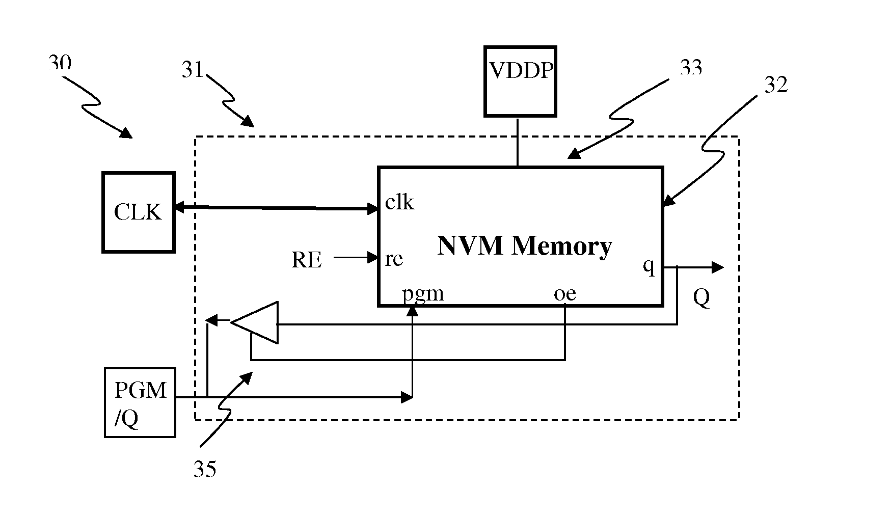
[0073]The invention relates to a low-pin-count non-volatile memory (NVM) having reduced area and footprint. In one embodiment, the low-pin-count non-volatile memory can use an interface that makes use of a minimum of three pins (i.e. VDDP, CLK, and PGM) external to an integrated circuit. In another embodiment, the low-pin-count non-volatile memory can use an interface that makes use of a minimum of two pins (i.e. VDDP and CLK) external to an integrated circuit. The interface not only can use only a few external pin but also can share several internal pins with the rest of integrated circuit to thereby reduce area and footprint. Moreover, if desired, the few external pins can be further multiplexed with the other pins so that no additional pins are needed. In one embodiment the interface can pertain to a low-pin-count OTP interface for an OTP memory so that the OTP memory can be easily integrated into an integrated circuit.

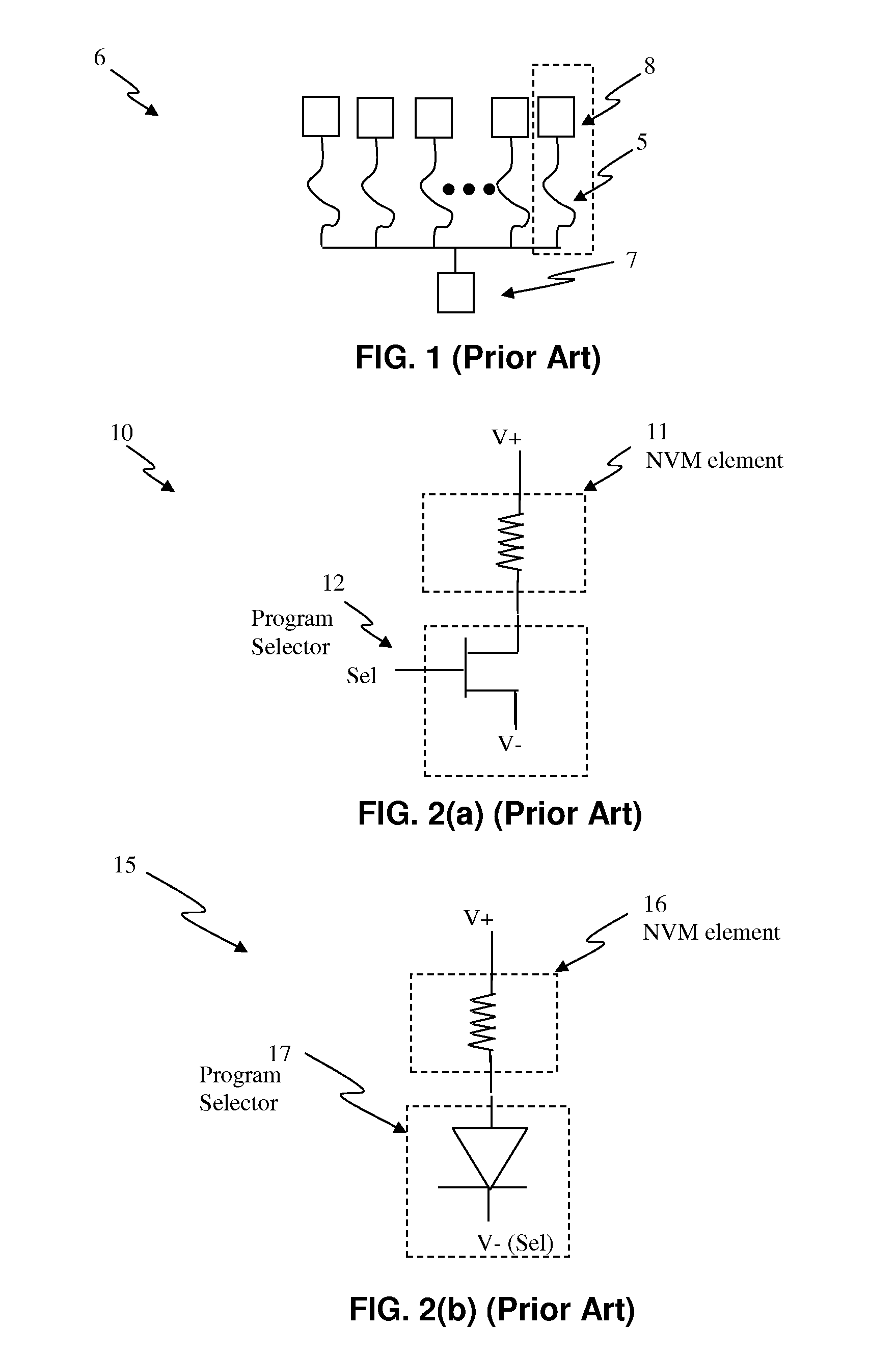
[0074]Simply employing a serial interface is not sufficient f...


PUM


Abstract

A low-pin-count non-volatile (NVM) memory with no more than two control signals that can at least program NVM cells, load data to be programmed into output registers, or read the NVM cells. At least one of the NVM cells has at least one NVM element coupled to at least one selector and to a first supply voltage line. The selector is coupled to a second supply voltage line and having a select signal. At least one of the selected NVM cells can be coupled to at least one output register. No more than two control signals can be used to select the at least one NVM cells in the NVM sequentially for programming the data into the at least one NVM cells or loading data into the at least one output registers controlled by the pulse of the first signal and voltage level and / or timing of the second signal. Programming into the NVM cells, or loading data into output registers, can be determined by the voltage levels of the first to the second supply voltage lines. Reading at least one of the NVM cells can be activated by a third signal or by detecting ramping of the first or the second supply voltage line.

Description

CROSS-REFERENCE TO RELATED APPLICATIONS[0001]This application is a continuation-in-part of U.S. patent application Ser. No. 13 / 288,843, filed on Nov. 3, 2011 and entitled “Low-Pin-Count Non-Volatile Memory Interface,” which incorporated herein as reference, and which claims priority benefit of U.S. Provisional Patent Application No. 61 / 409,539, filed on Nov. 3, 2010 and entitled “Circuit and System of A Low Pin Count One-Time-Programmable Memory,” which is hereby incorporated herein by reference.[0002]This application also claims priority benefit of U.S. Provisional Patent Application No. 61 / 806,914, filed on Mar. 31, 2013 and entitled “Low-Pin-Count Non-Volatile Memory Interface With Two Pins Only,” which is hereby incorporated herein by reference.[0003]This application is also related to U.S. patent application Ser. No. ______, filed on Mar. 31, 2014 and entitled “Low-Pin-Count Non-Volatile Memory Embedded in a Integrated Circuit Without Any Additional Pins For Access,” which is h...

Claims


Application Information

Patent Timeline
Patent Type & Authority Applications(United States)
IPC IPC(8): G11C8/18G11C17/16
CPCG11C17/16G11C8/18G11C2216/30G11C17/146G11C29/027G11C29/1201G11C29/46G11C16/16G11C16/26G11C16/32G11C16/10G11C29/022G11C7/10G11C17/00G11C13/004G11C13/0069G11C13/0097G11C16/0408G11C17/18
Inventor CHUNG, SHINE C.
Owner ATTOPSEMI TECH CO LTD
Why Eureka
Try Eureka