Organic Light Emitting Device

a light-emitting device and organic technology, applied in the direction of thermoelectric device junction materials, semiconductor devices, electrical apparatus, etc., can solve the problems of brightness and contrast limitations, and achieve the effect of preventing a smear

Active Publication Date: 2015-06-04
LG DISPLAY CO LTD
View PDF12 Cites 19 Cited by
  • Summary
  • Abstract
  • Description
  • Claims
  • Application Information

AI Technical Summary

Benefits of technology

[0021]An aspect of embodiments of the present invention is directed to provide an organic light emitting device that is able to prevent a smear from occurring at an edge of an active area, in a structure of multi protective layers.
[0022]Another aspect of embodiments of the present invention is directed to provide an organic light emitting device that is able to secure a flatness of an organic layer for preventing the organic layer from being thickly formed at an edge of an active area, in a structure of multi protective layers

Problems solved by technology

The LCD devices use a backlight as a separate light source, and have technical limitations in brightness and contrast.

Method used


Image

  • Organic Light Emitting Device
  • Organic Light Emitting Device
  • Organic Light Emitting Device

Examples


first embodiment

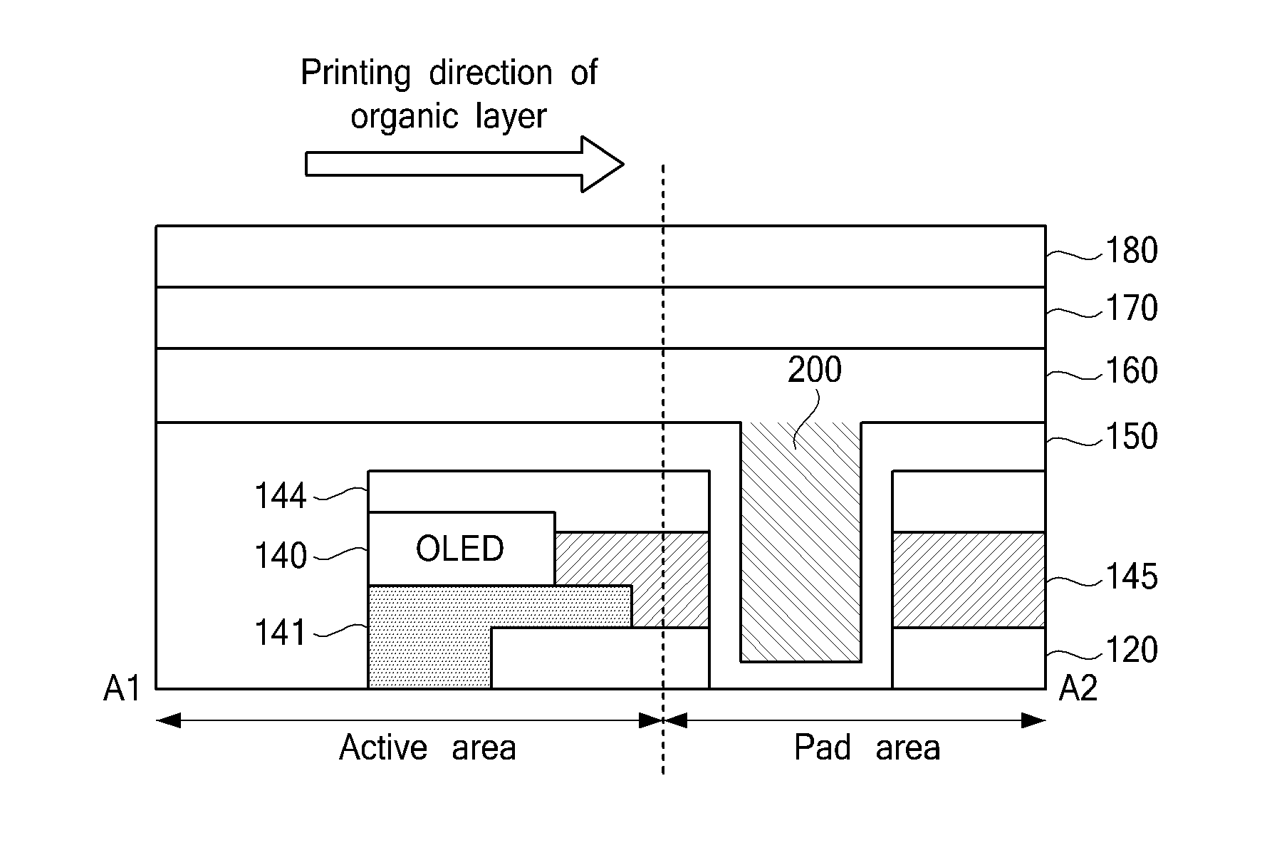
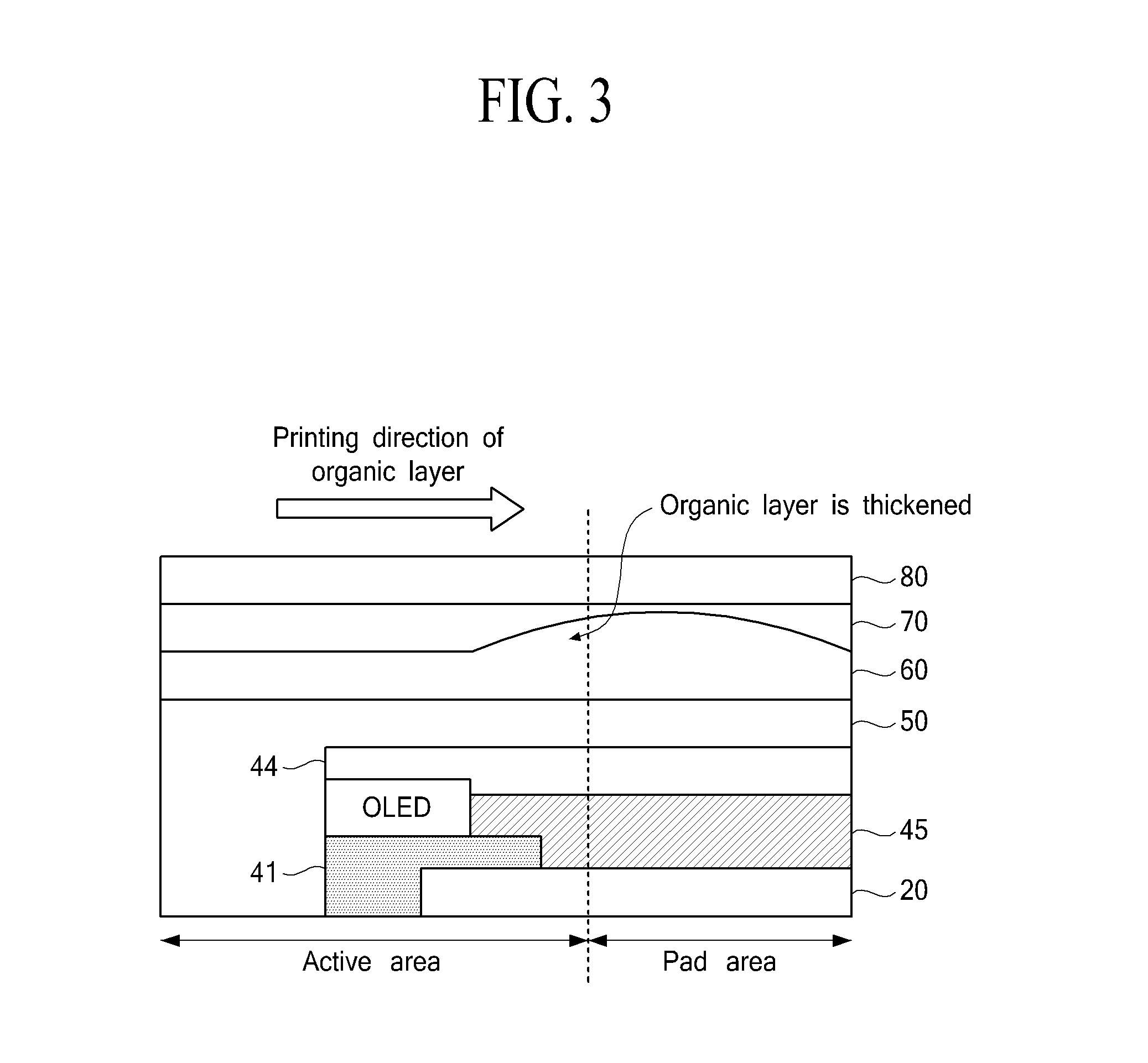
[0057]When the second protective layer 160 formed of an organic layer is thickly formed at an edge of the active area, an edge top can occur. In the organic light emitting device according to the present invention, the dam 200 is formed at a boundary between the active area and the pad area 110 so as to prevent the edge top from occurring. The dam 200 is formed to surround the active area. In the organic light emitting device according to the first exemplary embodiment, the second protective layer 160 is thereby not thickly formed at an edge of the active area, and prevents the edge top from occurring.

[0058]Here, the planarization layer 120 is formed to a thickness of 2 μm to 3 μm, and a bank 145 is formed to a thickness of 1 μm to 2 μm. The dam 200 is formed so that the planarization layer 120 and the bank 145 are not formed at the edge of the active area in a manufacturing process.

[0059]The dam 200 is formed with a groove at a portion that is separated from an outer portion of the...

second embodiment

[0071]When the second protective layer 160 formed of an organic layer is thickly formed at an edge of the active area, an edge top can occur. In the organic light emitting device according to the present invention, the dam 200 is formed at a boundary between the active area and the pad area so as to prevent the edge top from occurring.

[0072]Here, the planarization layer 120 is formed to a thickness of 2 μm to 3 μm, and a bank 145 is formed to a thickness of 1 μm to 2 μm. The dam 200 is formed so that the planarization layer 120 and the bank 145 are not formed at the edge of the active area in a manufacturing process.

[0073]As shown in FIG. 7A, a bank 145 is thickly formed at a first side (a left side of FIG. 6) of the edge of the active area. In this case, the bank 145 is thickly formed to a thickness of 4 μm to 6 μm, at a portion in which printing of the organic layer is started. When a bank is formed on the bank 145 in the pad area, the bank can prevent penetration of moisture from...


PUM


Abstract

An organic light emitting device includes a base substrate defining an active area and a pad area that surrounds the active area, an organic light emitting layer formed on the active area, a first protective layer formed to cover the active area, where the organic light emitting layer is formed, and the pad area, a second protective layer formed to cover the first protective layer, and a dam formed between the first protective layer and the second protective layer, wherein the dam is located at a boundary between the active area and the pad area and includes a groove that is positioned separate from an outer portion of the active area.

Description

[0001]The present application claims the benefit of the Korean Patent Application No. 10-2013-0149400 filed in Korea on Dec. 3, 2013, which is hereby incorporated by reference in its entirety.BACKGROUND[0002]1. Technical Field[0003]Embodiments of the present invention relate to an organic light emitting device that is able to secure a flatness of an organic layer and prevent a smear of an outer portion of an active area.[0004]2. Discussion of the Related Art[0005]Recently, liquid crystal display (LCD) devices have been widely used as flat panel display devices. The LCD devices use a backlight as a separate light source, and have technical limitations in brightness and contrast. To solve these problems, organic light emitting devices that self-emit light without a separate light source and have relatively better brightness and contrast than those of the LCD devices have been developed, and are being commercialized.[0006]The organic light emitting devices are divided into a passive ma...

Claims


Application Information

Patent Timeline
Patent Type & Authority Applications(United States)
IPC IPC(8): H01L51/52
CPCH01L51/5253H01L51/52H10K59/131H10K50/80H10K50/805H10K50/844H10K2102/302H10K59/805H10K59/122H10K50/852H10K2102/351
Inventor KIM, TAE-KYUNGKIM, BYOUNG CHULLEE, MYOUNG SOO
Owner LG DISPLAY CO LTD
Why Eureka
Try Eureka