Capacitance type touch panel, manufacturing method of the same, and input device
- Summary
- Abstract
- Description
- Claims
- Application Information
AI Technical Summary
Benefits of technology
Problems solved by technology
Method used
Image
Examples
first embodiment
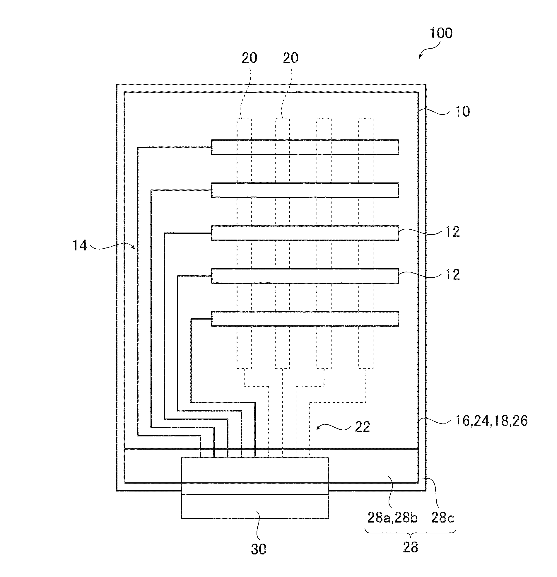
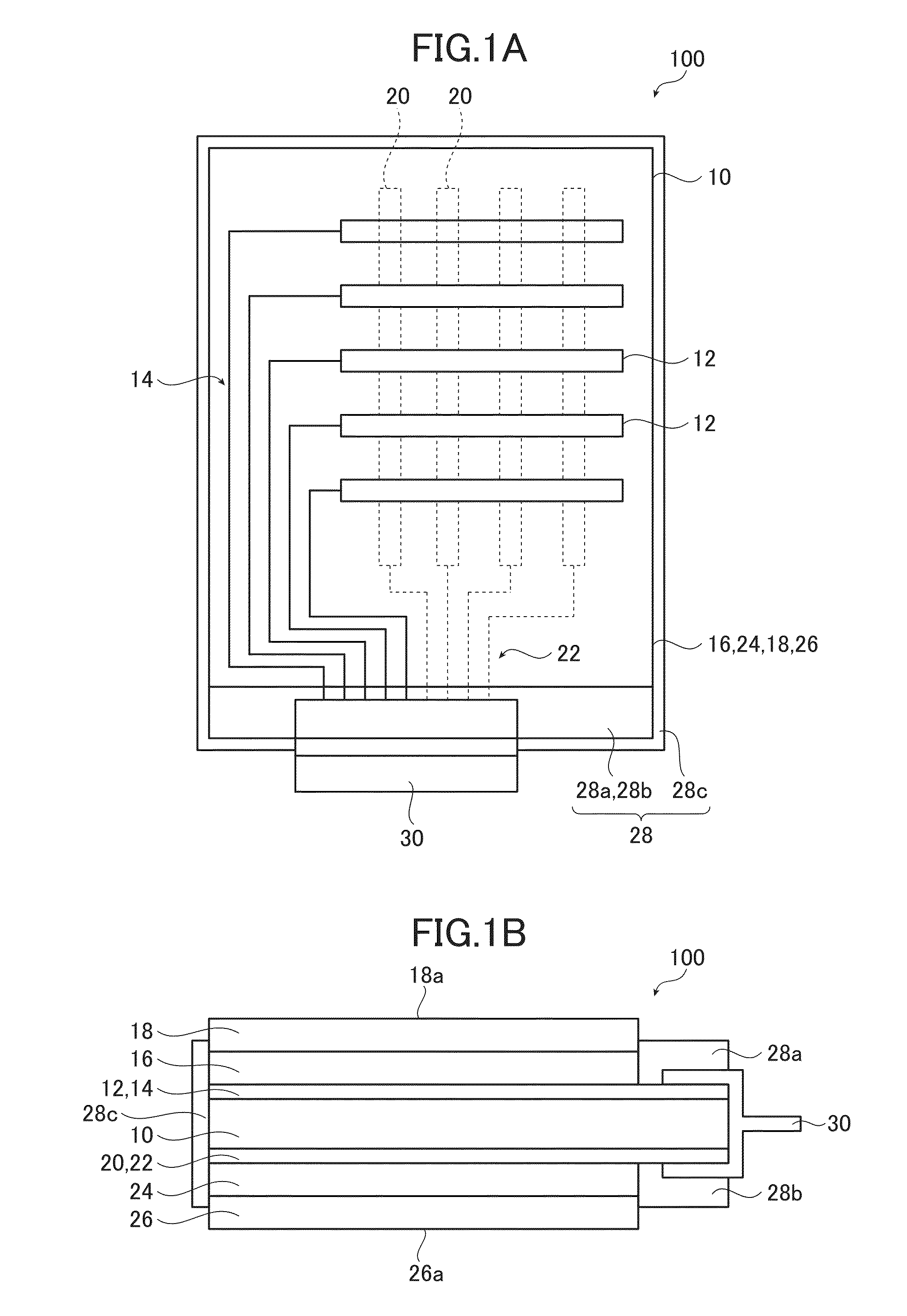
[0074]FIGS. 1A and 1B are schematic views of a first embodiment of the capacitance type touch panel of the present invention. FIG. 1A is a plan view of a capacitance type touch panel 100, and FIG. 1B is a cross-sectional view thereof. Herein, FIG. 1B is merely a schematic view for making it easy to understand the layer constitution of the capacitance type touch panel 100, and it does not accurately show the disposition of each layer.
[0075]As shown in FIGS. 1A and 1B, the capacitance type touch panel 100 includes an insulating layer 10; first electrode portions 12, first lead-out wiring portions 14, a first transparent resin layer 16, and a first protective substrate 18 that are disposed on the main surface (on the surface) at one side of the insulating layer 10; second electrode portions 20, second lead-out wiring portions 22, a second transparent resin layer 24, and a second protective substrate 26 that are disposed on the main surface (on the surface) at the other side of the insu...
second embodiment
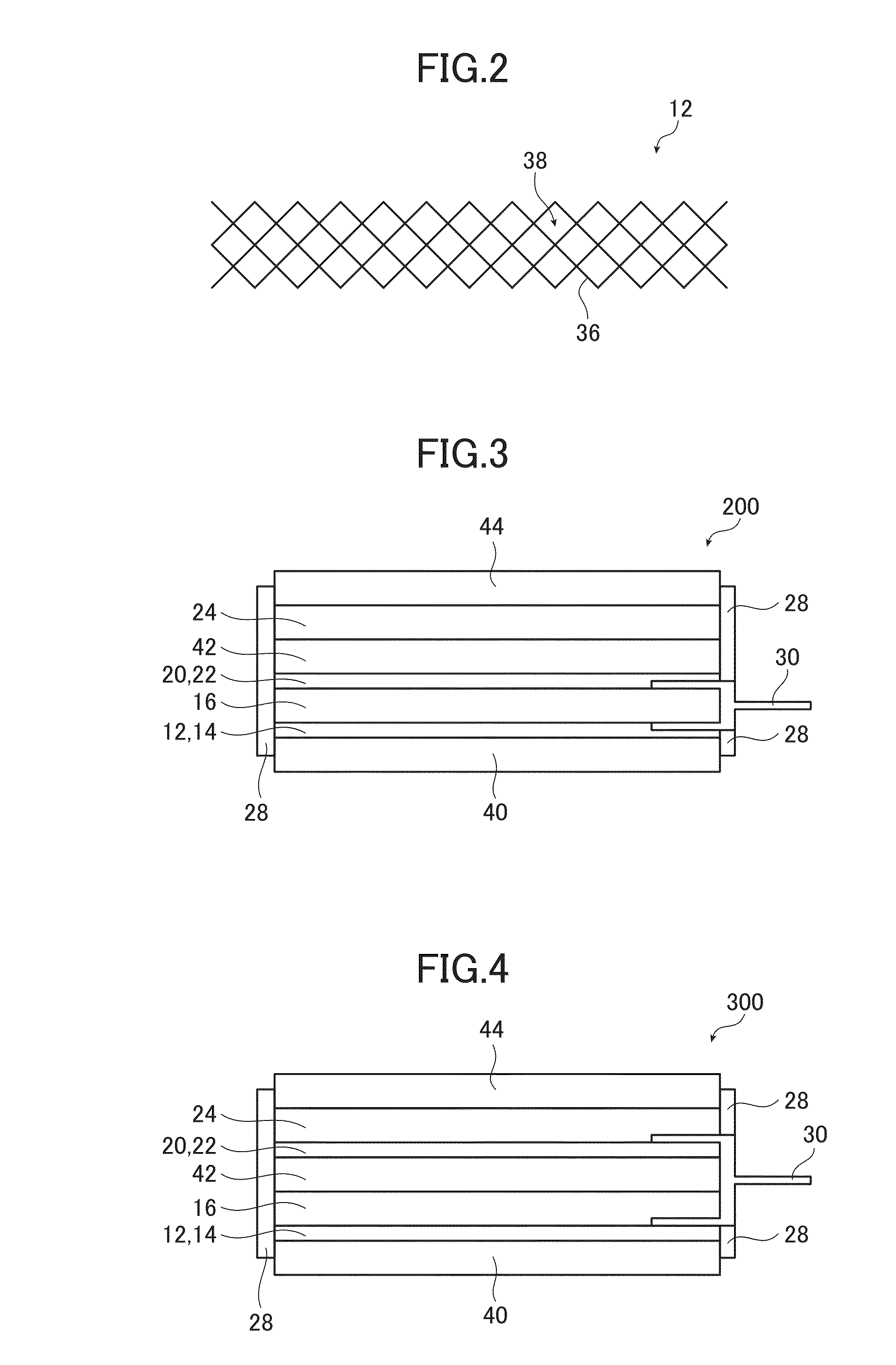
[0214]FIG. 3 is a cross-sectional view of a second embodiment of the capacitance type touch panel of the present invention. Herein, FIG. 3 is merely a schematic view for making it easy to understand the layer constitution of a capacitance type touch panel 200, and it does not accurately show the disposition of each layer.
[0215]As shown in FIG. 3, a capacitance type touch panel 200 includes a first insulating layer 40; the first electrode portions 12 and the first lead-out wiring portions 14 that are disposed on the main surface at one side of-the first insulating layer 40; the first transparent resin layer 16; the second electrode portions 20 and the second lead-out wiring portions 22; a second insulating layer 42; the second transparent resin layer 24; a protective substrate 44; the sealing layer 28; and the flexible printed wiring board 30.
[0216]The layers constituting the capacitance type touch panel 200 shown in FIG. 3 are the same as the layers constituting the capacitance type...
third embodiment
[0220]FIG. 4 is a cross-sectional view of a third embodiment of the capacitance type touch panel of the present invention. Herein, FIG. 4 is merely a schematic view for making it easy to understand the layer constitution of a capacitance type touch panel 300, and it does not accurately show the disposition of each layer.
[0221]As shown in FIG. 4, the capacitance type touch panel 300 includes the first insulating layer 40; the first electrode portions 12 and the first lead-out wiring portions 14 that are disposed on the main surface of one side of the first insulating layer 40; the first transparent resin layer 16; the second insulating layer 42; the second electrode portions 20 and the second lead-out wiring portions 22; the second transparent resin layer 24; the protective substrate 44; the sealing layer 28; and the flexible printed wiring board 30.
[0222]The layers constituting the capacitance type touch panel 300 shown in FIG. 4 are the same as the layers constituting the capacitan...
PUM
 Abstract
Description
Claims
Application Information


