Method for manufacturing semiconductor device

Active Publication Date: 2015-06-25
SEMICON MFG INT (SHANGHAI) CORP
View PDF1 Cites 4 Cited by
  • Summary
  • Abstract
  • Description
  • Claims
  • Application Information

AI Technical Summary

Benefits of technology

[0021]Embodiments of the invention may enable effective protection of work function layers and/or effective formation of metal gate members in manufacturing of semiconductor devices. Therefore, satisfactory quality and/or performance of work fun

Problems solved by technology

Nevertheless, chemicals used and/or generated during processing of the SiN spacers may substantially obstruct the removal of the polysilicon dummy gate and/or may cause an undesirable trapezoidal profile of a space for receiving metal gate material.
The trapezoidal profile may undesirably affect the filling of the metal gate material and formation of the me

Method used


Image

  • Method for manufacturing semiconductor device
  • Method for manufacturing semiconductor device
  • Method for manufacturing semiconductor device

Examples


Embodiment Construction

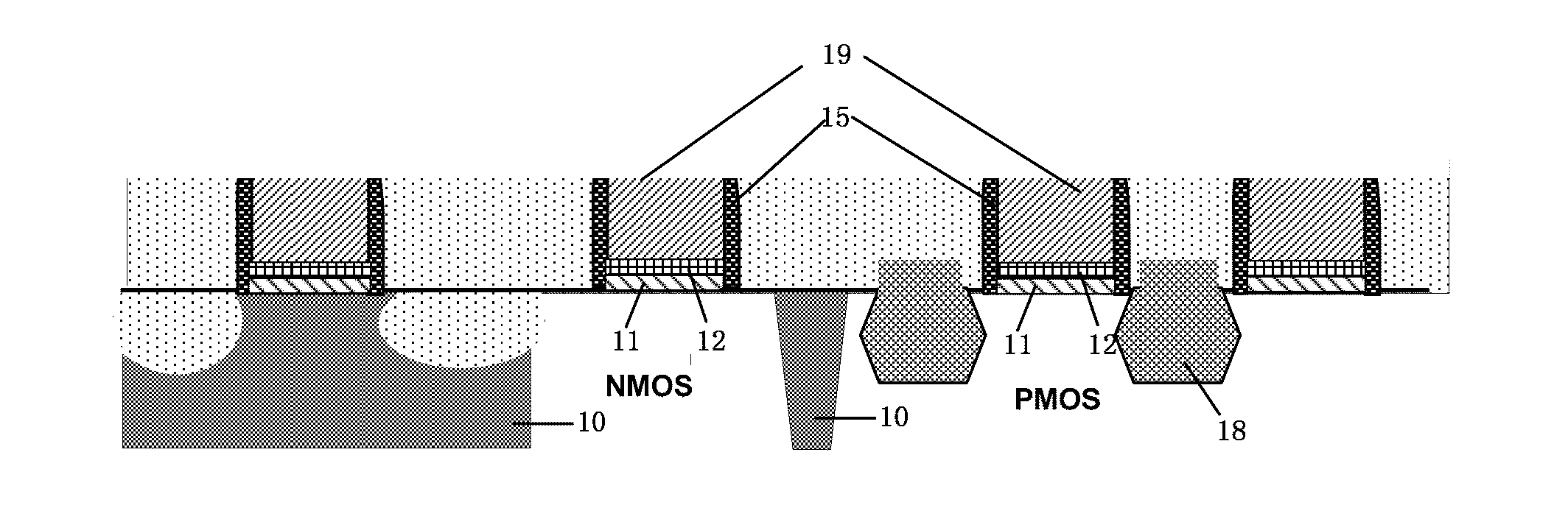
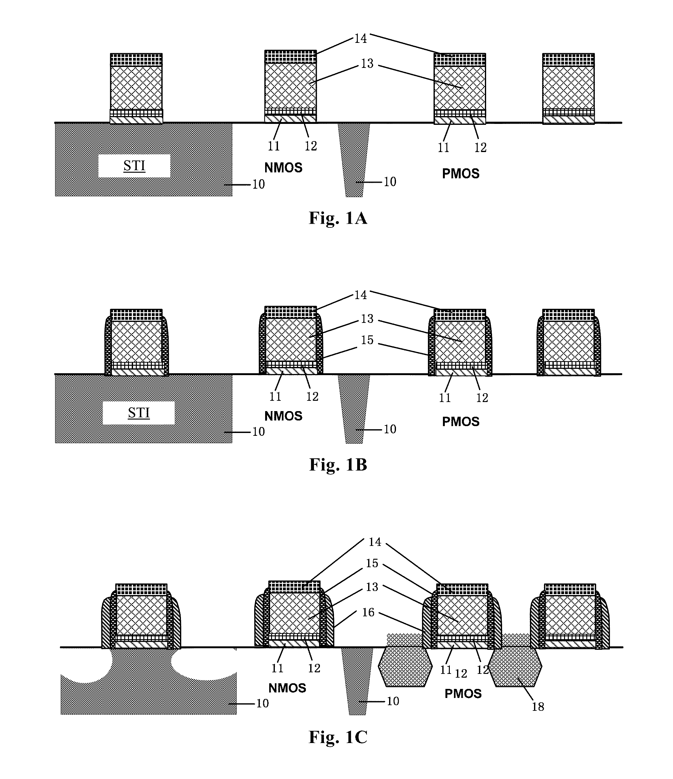
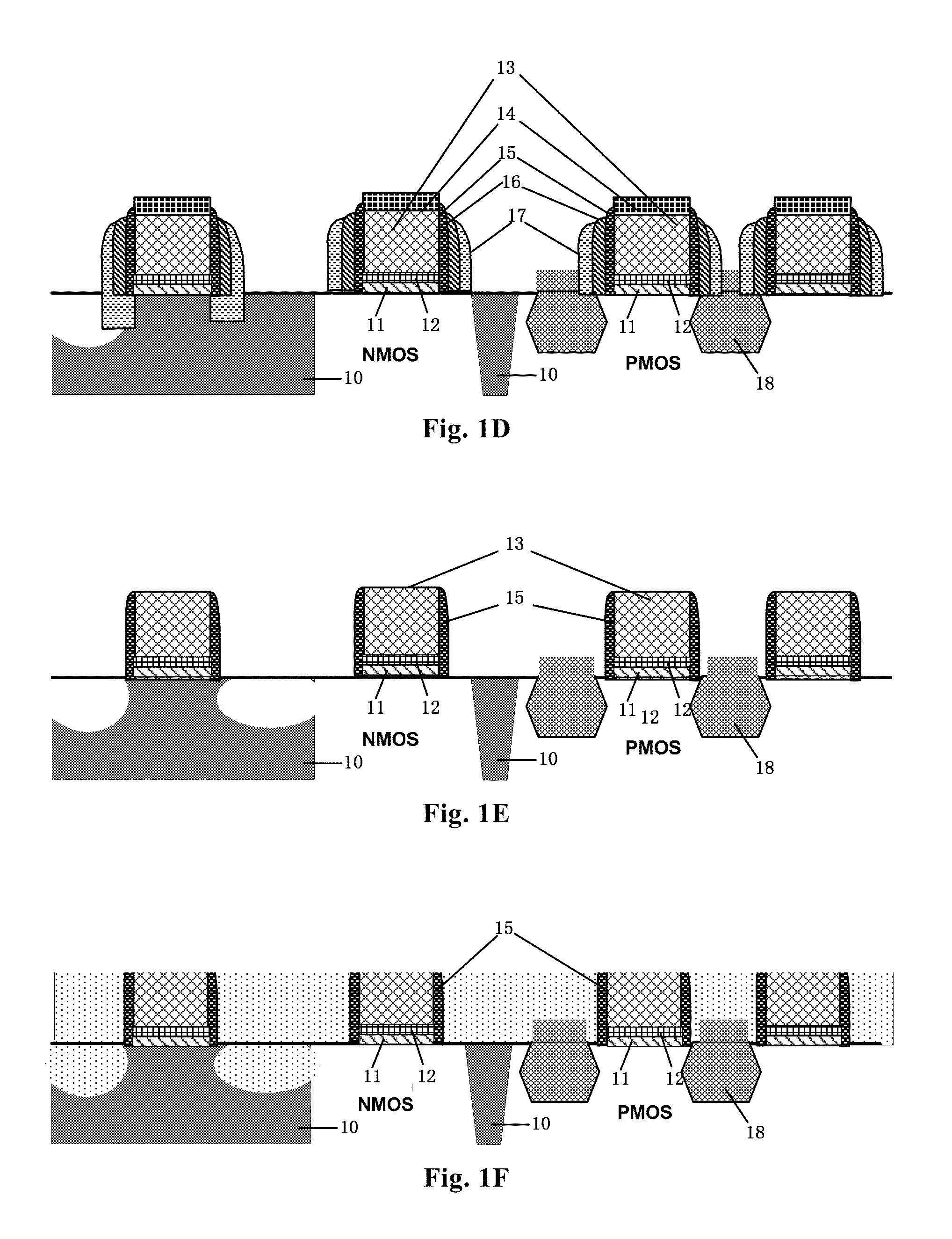
[0027]Example embodiments of the present invention are described with reference to the accompanying drawings. In the following description, numerous specific details are set forth in order to provide thorough understanding of the present invention. Embodiments of the present invention may be practiced without some or all of these specific details. Well known process steps and / or structures may not have been described in detail in order to not unnecessarily obscure the present invention.

[0028]Various embodiments, including methods and techniques, are described in this disclosure. It should be kept in mind that the invention might also cover an article of manufacture that includes a non-transitory computer readable medium on which computer-readable instructions for carrying out embodiments of the inventive technique are stored. The computer readable medium may include, for example, semiconductor, magnetic, opto-magnetic, optical, or other forms of computer readable medium for storing ...


PUM


Abstract

A method for manufacturing a semiconductor device may include forming a gate structure that includes a dummy gate member on a substrate. The method may further include forming two first-type spacers such that the dummy gate member is positioned between the first-type spacers. The method may further include forming two second-type spacers such that the first-type spacers are positioned between the second-type spacers. The method may further include forming two third-type spacers such that the second-type spacers are positioned between the third-type spacers. The method may further include performing etch to remove the third-type spacers and to at least partially remove the second-type spacers. The method may further include removing at least a portion of the dummy gate member to form a space between remaining portions of the first-type spacers. The method may further include providing a metal material in the space for forming a metal gate member.

Description

CROSS-REFERENCE TO RELATED APPLICATION[0001]This application claims priority to and benefit of Chinese Patent Application No. 201310706433.4, filed on 20 Dec. 2013, the Chinese Patent Application being incorporated herein by reference in its entirety.BACKGROUND OF THE INVENTION[0002]The present invention is related to a method for manufacturing a semiconductor device. For example, the present invention may be related to a method for manufacturing a high-k metal gate (HKMG) semiconductor device, i.e., a semiconductor device that includes a high-k member (with a dielectric constant higher than the dielectric constant of silicon dioxide or 2.5) and a metal gate member.[0003]Manufacturing of an HKMG semiconductor device may involve minimization of oxygen diffusion and removal of a polysilicon dummy gate. For minimizing oxygen diffusion, spacers (e.g., offset spacers) in the device may be formed of silicon nitride (SiN). Nevertheless, chemicals used and / or generated during processing of ...

Claims


Application Information

Patent Timeline
IPC IPC(8): H01L21/8238H01L29/49
CPCH01L29/49H01L21/823864H01L21/823807H01L21/823814H01L21/823878H01L29/4966H01L29/517H01L29/6653H01L29/66545H01L29/66636H01L29/7848H01L29/165
Inventor WEI, QINGSONGYU, SHUKUN
Owner SEMICON MFG INT (SHANGHAI) CORP
Why Eureka
Try Eureka