Coating and developing apparatus and method
a technology of developing apparatus and coating, which is applied in the direction of electrical apparatus, printing, instruments, etc., can solve the problems of lowering the operation efficiency of the apparatus, and achieve the effect of reducing the lowering of the operation efficiency of the coating and the increase of the footprint of the processing block
- Summary
- Abstract
- Description
- Claims
- Application Information
AI Technical Summary
Benefits of technology
Problems solved by technology
Method used
Image

Examples
first embodiment
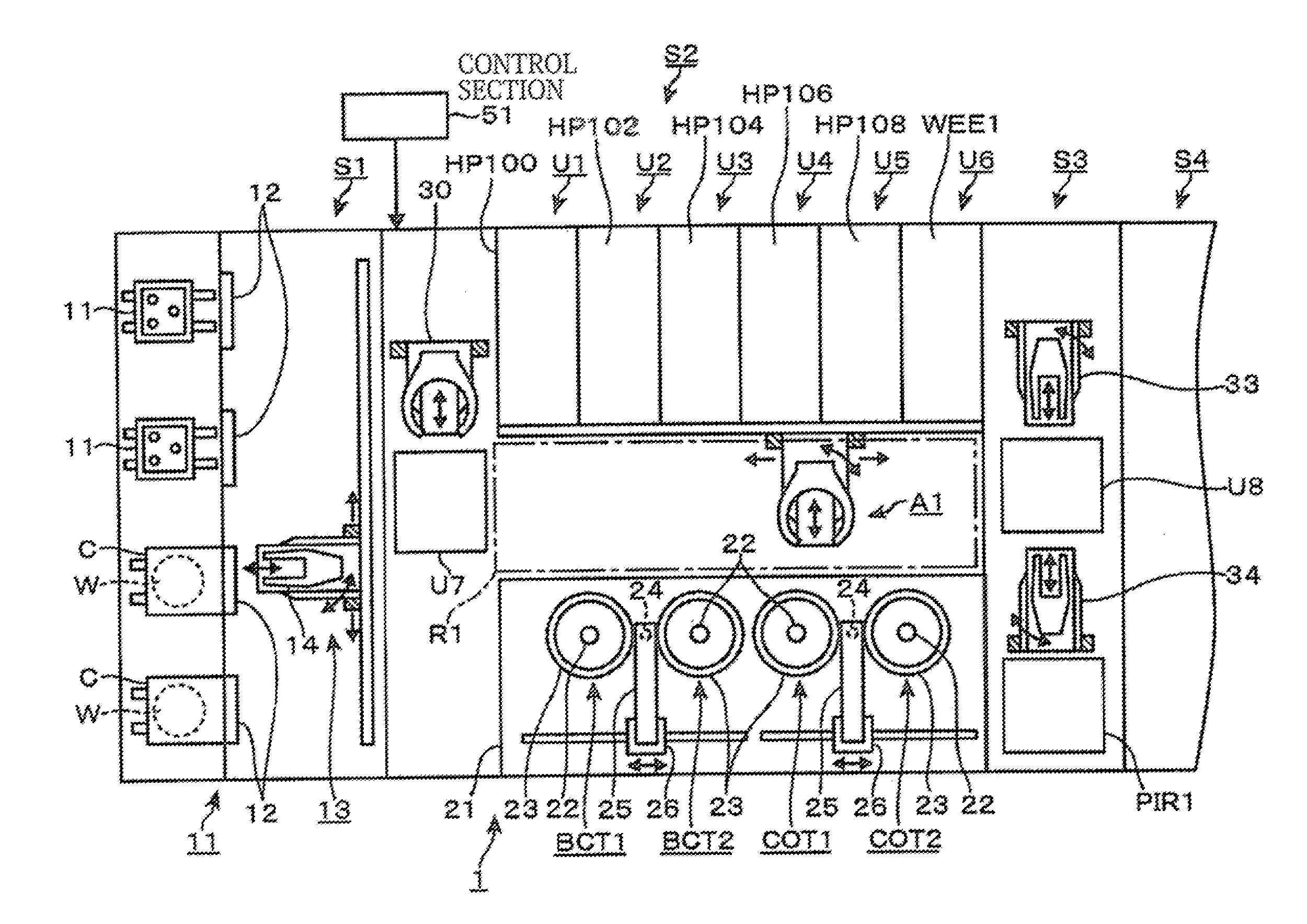
[0053]The construction of a coating and developing apparatus will now be described with reference to FIGS. 1 to 3. The coating and developing apparatus 1 includes a carrier block S1 for receiving and delivering carriers C in each of which a plurality of, for example 25, wafers W are hermetically housed, a processing block S2 for performing processing of the wafers W, and an interface block S3, the blocks being arrayed linearly, To the interface block S3 is connected to an exposure apparatus S4 for performing immersion exposure. For the convenience of description of positional relationships in a plan view of the apparatus, the right side of FIG. 1 is hereinafter referred to as “anterior”, the left side as “posterior”, the upper side as “left”, and the lower side as “right”.
[0054]The carrier block S1 includes stages 11 for placing the carriers C thereon, shutters 12 provided in a wall in front of the stages 11, and a transfer arm 13 for taking wafers W out of the carriers C via the sh...
second embodiment
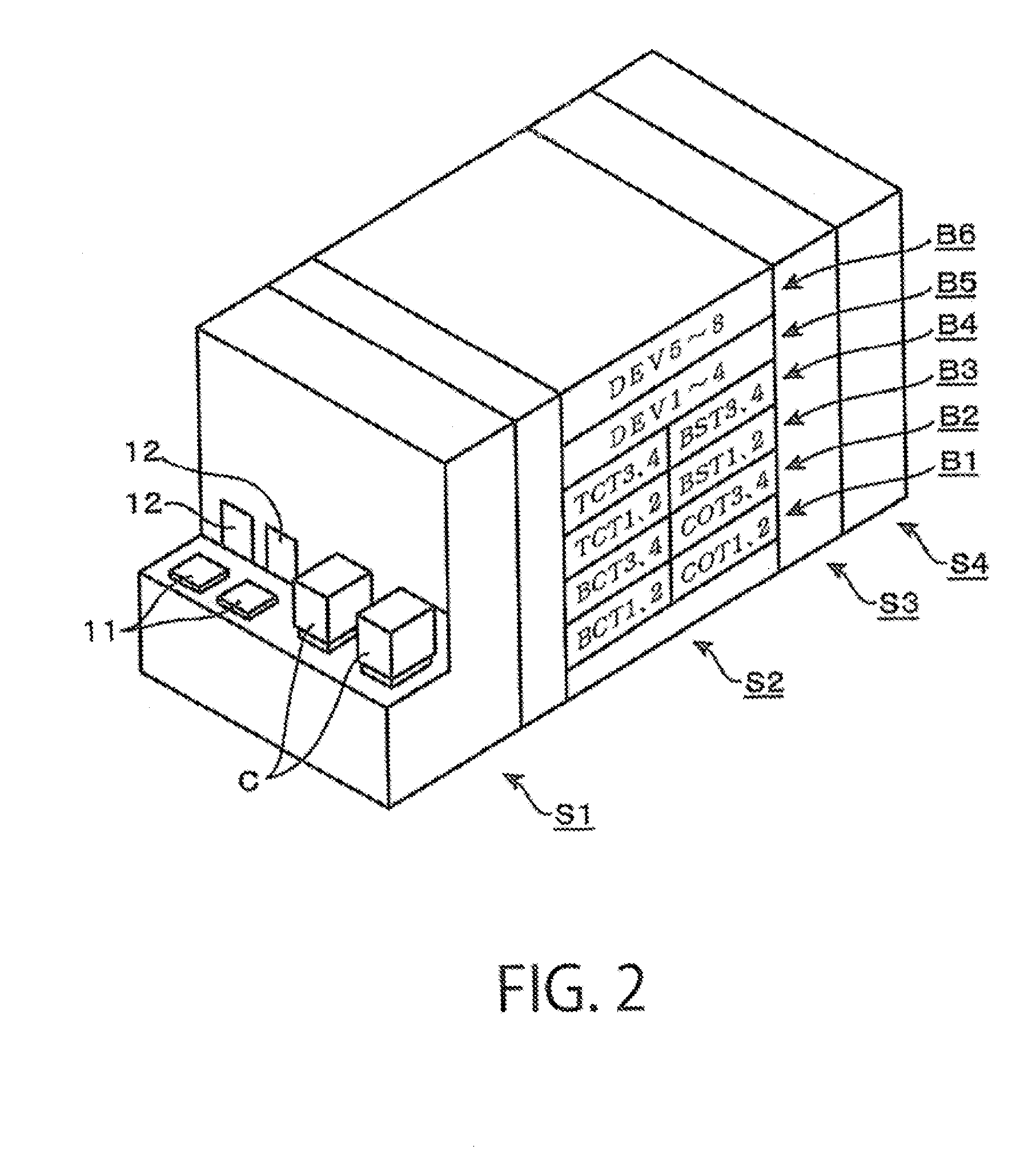
[0139]The processing block 5 of a coating and developing apparatus according to a second embodiment will now be described with reference to FIG. 17. In the processing block S5, a pair of unit blocks B1, B2 including antireflection film-forming modules (BCT1 to BCT8), a pair of unit blocks B3, B4 including resist film-forming modules (COT1 to COT8), and a pair of unit blocks B5, B6 including developing modules (DEV1 to DEV8) each constitute a doubled unit block. Each of the unit blocks B1 to B4 of the processing block S5 is the same in the mechanical construction as each of the unit blocks B1 to B4 of the processing block S2, though they differ in liquid processing preformed in their liquid processing modules. The unit blocks B1, B2, B3 and B4 of the processing block S5 are provided with the antireflection film-forming modules BCT1 to BCT4, the antireflection film-forming modules BCT5 to BCT8, the resist film-forming modules COT1 to COT4 and the resist film-forming modules COT5 to CO...
third embodiment
[0144]The processing block S6 of a coating and developing apparatus according to a third embodiment will now be described with reference to FIG. 18. The processing block S6 includes 8 unit blocks stacked in 8 stages. The eight unit blocks are herein referred to as E1, E2, E3, E4, E5, E6, E7 and E8 in the stacking order from the lowest one. In the processing block S6, the unit blocks E1 to E4 have the same construction as the unit blocks B1 to B4 of the processing block S5. The unit blocks E5 and E6, stacked on the unit block E4, have the same construction and are provided with protective film-forming modules TCT1 to TCT4 and TCT5 to TCT8, respectively, Each of the unit blocks E5 and E6 has the same mechanical construction as each of the unit blocks E1 to E4 except that different processing is performed by the liquid processing modules. The unit blocks E7, E8, stacked on the unit block E5, have the same construction as the unit blocks B5, B6 of the processing block S2 of the first em...
PUM
| Property | Measurement | Unit |
|---|---|---|
| centrifugal force | aaaaa | aaaaa |
| rotation | aaaaa | aaaaa |
| viscosity | aaaaa | aaaaa |
Abstract
Description
Claims
Application Information
 - R&D
- Intellectual Property
- Life Sciences
- Materials
- Tech Scout
- Unparalleled Data Quality
- Higher Quality Content
- 60% Fewer Hallucinations
Browse by: Latest US Patents, China's latest patents, Technical Efficacy Thesaurus, Application Domain, Technology Topic, Popular Technical Reports.
© 2025 PatSnap. All rights reserved.Legal|Privacy policy|Modern Slavery Act Transparency Statement|Sitemap|About US| Contact US: help@patsnap.com