Thermally enhanced low parasitic power semiconductor package

Active Publication Date: 2011-03-31
TEXAS INSTR INC
View PDF11 Cites 39 Cited by
  • Summary
  • Abstract
  • Description
  • Claims
  • Application Information

AI Technical Summary

Benefits of technology

[0009]In realizing the shortcomings of conventional device designs, the inventors have developed a new semiconductor package design and method of assembly which provides dual heat dissipation and allows attachment to generally flat surfaces of both source-side and drain-side die pads while avoiding the use of a flip chip process. Thus the connection of the device to the leadframe can be performed with conventional pick-and-place equipment to increase device throughput using a pattern recognition system (PRS) to align the chip with the leadframe, which is not possible in a flip-chip process. Also, since the surfaces of both the source-side and drain-side leadframe subassemblies are generally flat across both X- and Y-directions, the thickness of the drain-side leadframe can be customized for the operating characteristics of the die. For example, a thicker drain-side leadframe subassembly can be used for higher power devices to more efficiently dissipate heat.
[0010]In one embodiment, a drain-side leadframe subass

Problems solved by technology

Devices such as power metal oxide semiconductor field effect transistors (MOSFETs)

Method used


Image

  • Thermally enhanced low parasitic power semiconductor package
  • Thermally enhanced low parasitic power semiconductor package
  • Thermally enhanced low parasitic power semiconductor package

Examples


Embodiment Construction

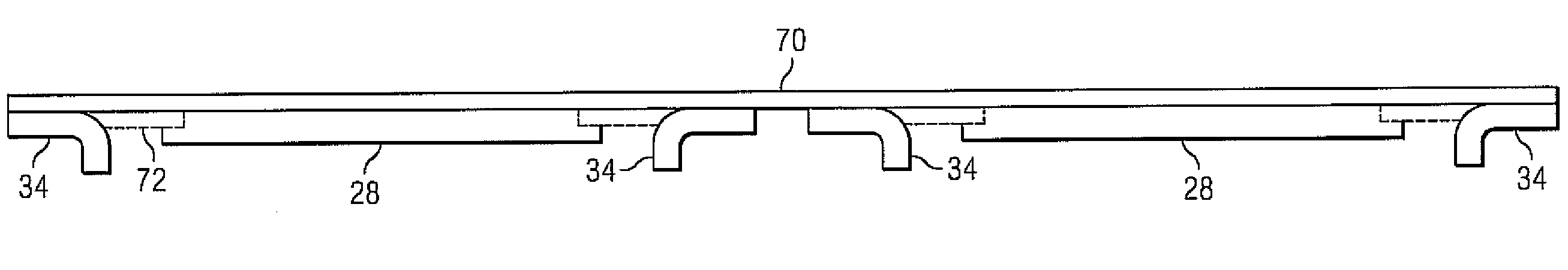
[0006]In contemplating conventional dual cool package assemblies, the inventors have realized that flip chip processing of power devices is a slow process with a low device throughput, which increases costs, and is not desirable. For example, conventional die attach methods which do not use flip chip processing can remove a die from a wafer carrier using a pick-and-place apparatus, and attach the back of the die to the leadframe pad. Throughput with a non-flip chip process using conventional equipment can be as high as 4,800 units per hour (UPH). In contrast, flip chip processing requires removal of the die from the wafer carrier, inversion of the die, then attachment of the front of the chip to the leadframe. With flip chip processing, device throughput can decrease to about 1,800 UPH, thereby requiring more than twice the equipment to produce the same number of devices. Even though flip chip processing is not desirable, conventional designs of dual cool packages require the use of...


PUM


Abstract

A method and structure for a dual heat dissipating semiconductor device. A method includes attaching a drain region on a first side of a die, such as a power metal oxide semiconductor field effect transistor (MOSFET) to a first leadframe subassembly. A source region and a gate region on a second side of the die are attached to a second leadframe subassembly. The first leadframe subassembly is attached to a third leadframe subassembly, then the device is encapsulated or otherwise packaged. An exposed portion of the first leadframe subassembly provides an external heat sink for the drain region, and the second leadframe subassembly provides external heat sinks for the source region and the gate region, as well as output leads for the gate region. The third leadframe subassembly provides output leads for the drain region.

Description

FIELD OF THE INVENTION[0001]This invention relates to the field of semiconductor devices, and more particularly to a low parasitic, dual heat dissipating semiconductor package and method for forming the package.BACKGROUND OF THE INVENTION[0002]During the design of packaging for semiconductor chips, various aspects such as heat dissipation and electrical performance must be considered. Devices such as power metal oxide semiconductor field effect transistors (MOSFETs) are susceptible to overheating during device operation due to high current cycling.[0003]To reduce the impact of high thermal output during operation, dual heat dissipating package (i.e. “dual cool”) assemblies have been developed. These packages can include a thermally and electrically conductive leadframe subassembly which connects to a source and gate side of the power MOSFET, and a thermally and electrically conductive bridge or clip which connects to a drain side of the power MOSFET. Portions of the leadframe and cl...

Claims


Application Information

Patent Timeline
IPC IPC(8): H01L23/495H01L21/50
CPCH01L23/3107H01L23/49537H01L23/49562H01L24/34H01L2924/01029H01L2924/01082H01L2924/01033H01L2924/1306H01L2924/014H01L23/49568H01L2924/13091H01L2224/32245H01L2924/00H01L2924/181H01L2224/8385H01L2224/8485H01L24/40H01L24/84H01L2924/00012H01L2924/00014
Inventor LOPEZ, OSVALDO JORGENOQUIL, JONATHAN ALMERIAHERBSOMMER, JUAN ALEJANDRO
Owner TEXAS INSTR INC
Why Eureka
Try Eureka