Systems and Methods for Hard Error Reduction in a Solid State Memory Device

a solid-state memory and hard-drive technology, applied in the field of solid-state memory, can solve the problems that the data in the solid-state storage device decays over time, and the enhanced error-correction circuitry may not be able to correct all mis-programming errors, so as to reduce the bit error rate of the read data

Active Publication Date: 2015-08-06
SEAGATE TECH LLC
View PDF1 Cites 11 Cited by
  • Summary
  • Abstract
  • Description
  • Claims
  • Application Information

AI Technical Summary

Benefits of technology

[0006]Various embodiments of the present invention provide methods for writing data to a solid state memory device. The methods include: programming a multi-bit cell of a memory device with a first value selected based upon a first bit value; reading the cell of the memory device using a currently modified reference value to yi

Problems solved by technology

Data in a solid state storage device decays over time requiring more error correction capability over time.
However, such enhan

Method used


Image

  • Systems and Methods for Hard Error Reduction in a Solid State Memory Device
  • Systems and Methods for Hard Error Reduction in a Solid State Memory Device
  • Systems and Methods for Hard Error Reduction in a Solid State Memory Device

Examples


Embodiment Construction

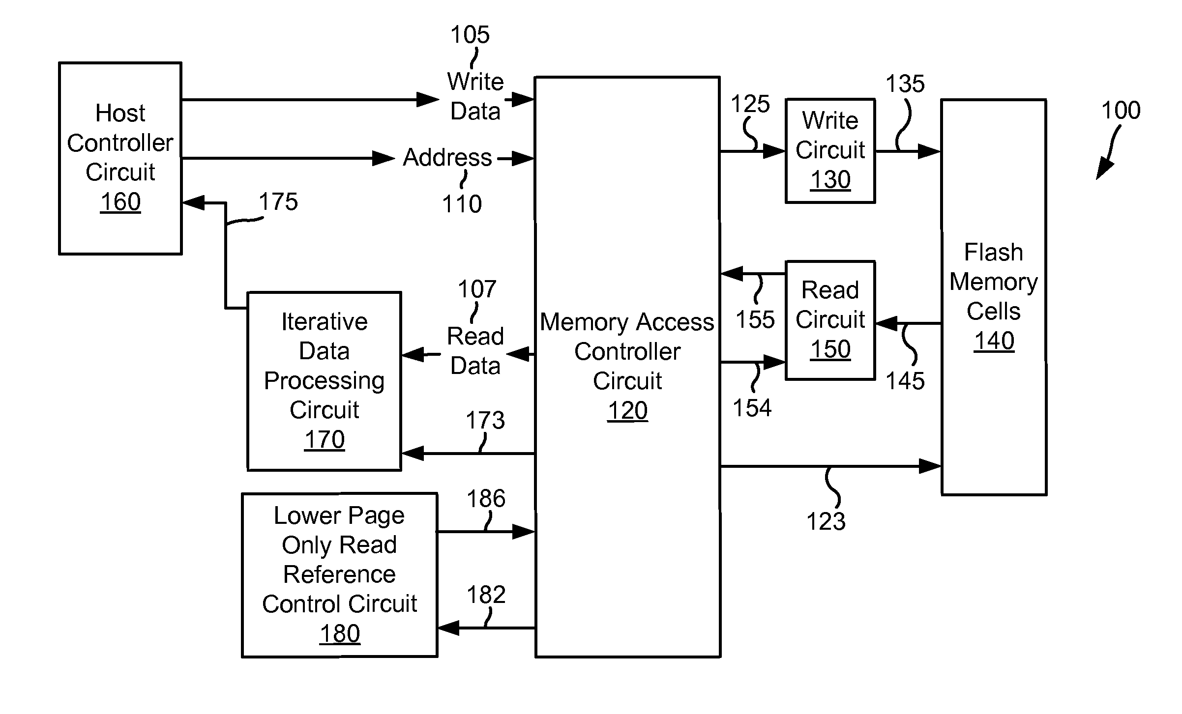
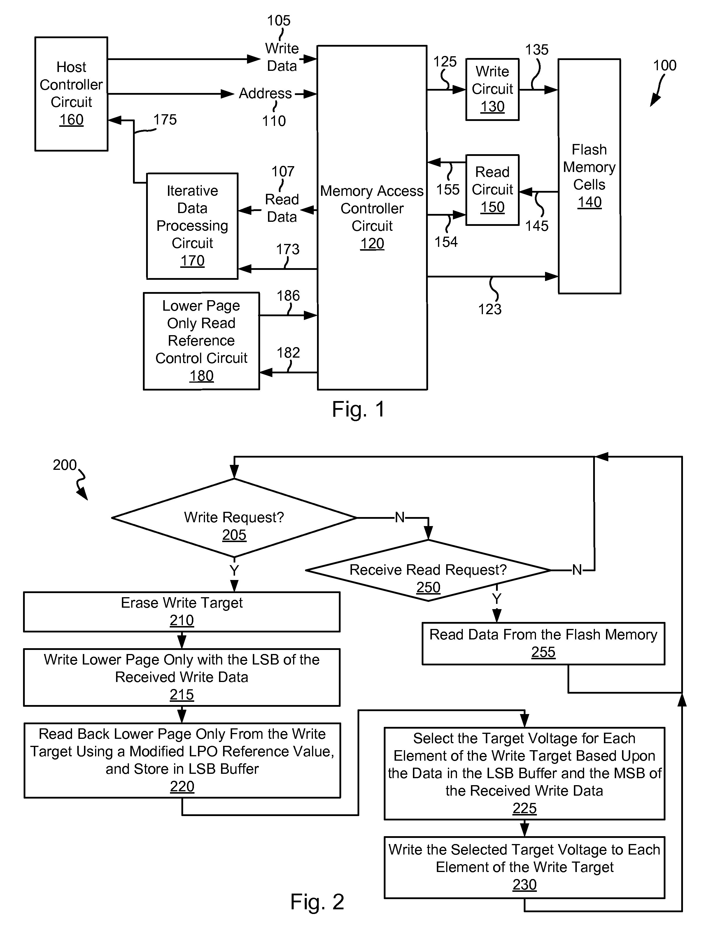
[0016]Systems and method relating generally to solid state memory, and more particularly to systems and methods for reducing errors in a solid state memory.

[0017]Various embodiments of the present invention provide methods for writing data to a solid state memory device. The methods include: programming a multi-bit cell of a memory device with a first value selected based upon a first bit value; reading the cell of the memory device using a currently modified reference value to yield a read data; programming the multi-bit cell of the memory device with a second value selected based upon a combination of a second bit value and the read data; and generating the currently modified reference value such that it yields a reduced bit error rate of the read data compared with a previous modified reference value.

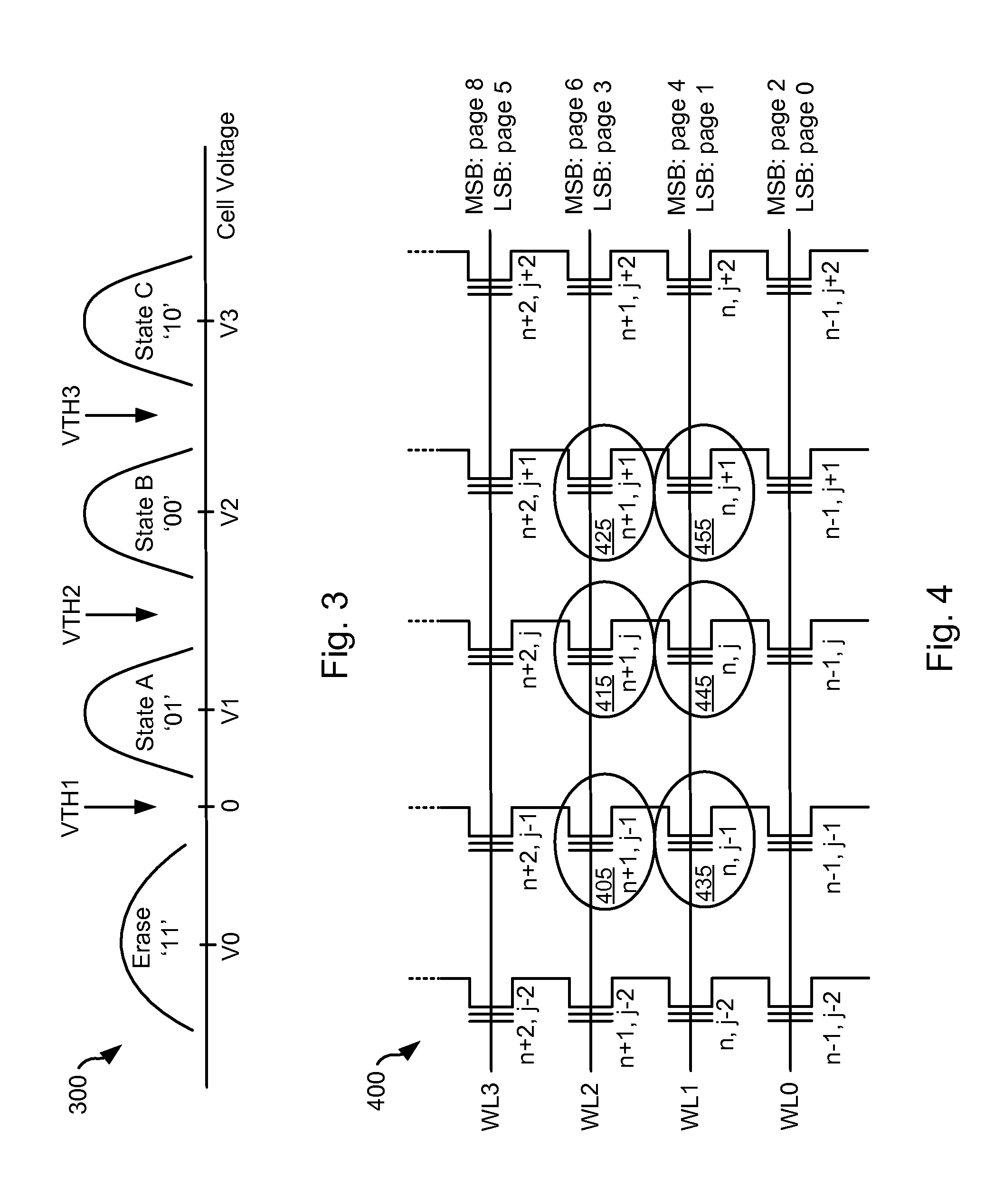
[0018]In some instances of the aforementioned embodiments, generating the currently modified reference value includes: programming two or more cells of a selected region of the memor...


PUM


Abstract

Systems and method relating generally to solid state memory, and more particularly to systems and methods for reducing errors in a solid state memory.

Description

CROSS REFERENCE TO RELATED APPLICATIONS[0001]The present application claims priority to (is a non-provisional of) U.S. Pat. App. No. 61 / 936,599 entitled “Systems and Methods for Hard Error Reduction in a Solid State Memory Device”, and filed Feb. 6, 2014 by Wu et al. The entirety of the aforementioned provisional patent application is incorporated herein by reference for all purposes.FIELD OF THE INVENTION[0002]Systems and method relating generally to solid state memory, and more particularly to systems and methods for reducing errors in a solid state memory.BACKGROUND[0003]Data in a solid state storage device decays over time requiring more error correction capability over time. To correct additional errors, enhanced error correction circuitry may be employed. However, such enhanced error correction circuitry may not be able to correct all mis-programming errors occurring in a solid state memory device.[0004]Hence, for at least the aforementioned reasons, there exists a need in the...

Claims


Application Information

Patent Timeline
IPC IPC(8): G06F11/10G11C29/52
CPCG11C29/52G06F11/1068G06F3/0619G06F3/0688G06F11/1012G06F11/1072G11C7/14G11C11/5628G11C11/5642G11C13/0033G11C16/0483G11C16/10G11C16/26G11C16/34G11C16/3404G11C16/3427G11C16/349G11C29/021G11C29/028G11C29/42G11C2029/0411
Inventor WU, YUNXIANGCAI, YUHARATSCH, ERICH F.
Owner SEAGATE TECH LLC
Why Eureka
Try Eureka