Electronic device and method of manufacturing the same

a technology of electronic devices and manufacturing methods, applied in the direction of electric variable regulation, process and machine control, instruments, etc., can solve the problems of difficult noise within the frequency range, severe impact on the operation of the first circuit,

Active Publication Date: 2015-08-27
NXP BV
View PDF18 Cites 4 Cited by
  • Summary
  • Abstract
  • Description
  • Claims
  • Application Information

AI Technical Summary

Benefits of technology

[0026]In particular when the first circuit comprises an NFC communication interface, operation of the first circuit will not be significantly

Problems solved by technology

In the present context, the term “the first circuit being susceptible to power supply noise within a predetermined frequency range” may particularly denote that the operation of the first circuit may suffer severe impact or even be impossible in case of power supply no

Method used


Image

  • Electronic device and method of manufacturing the same
  • Electronic device and method of manufacturing the same
  • Electronic device and method of manufacturing the same

Examples


Embodiment Construction

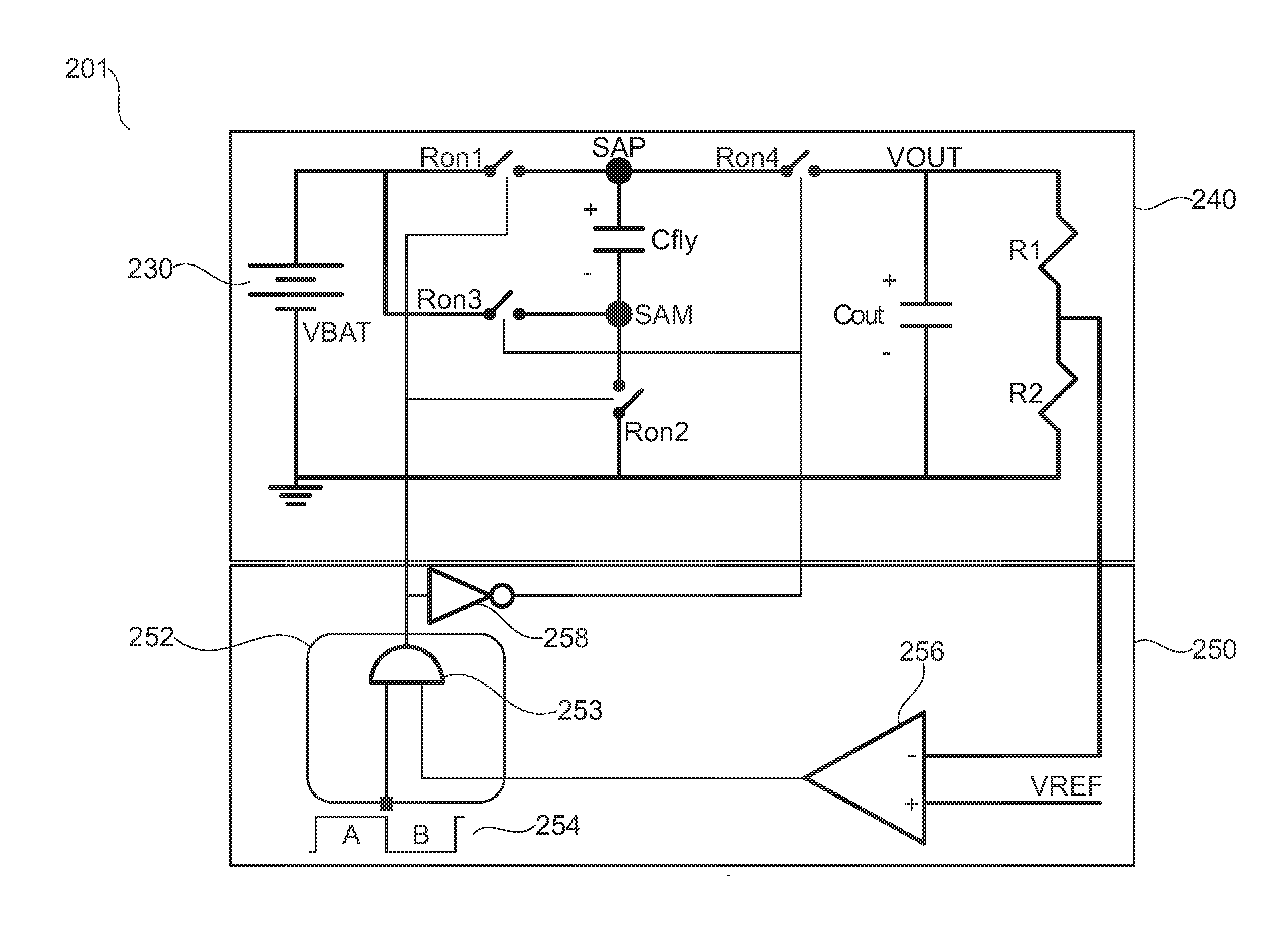
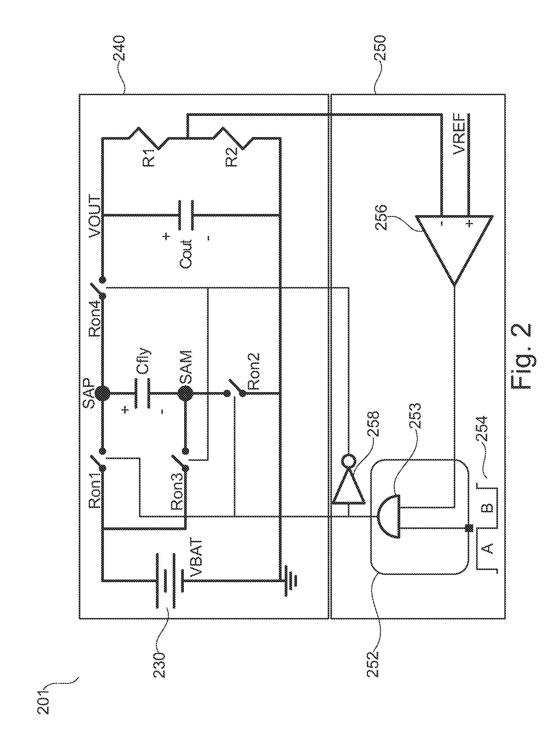
[0036]The illustration in the drawing is schematic. It is noted that in different figures, similar or identical elements are provided with the same reference signs or with reference signs, which differ only within the first digit.

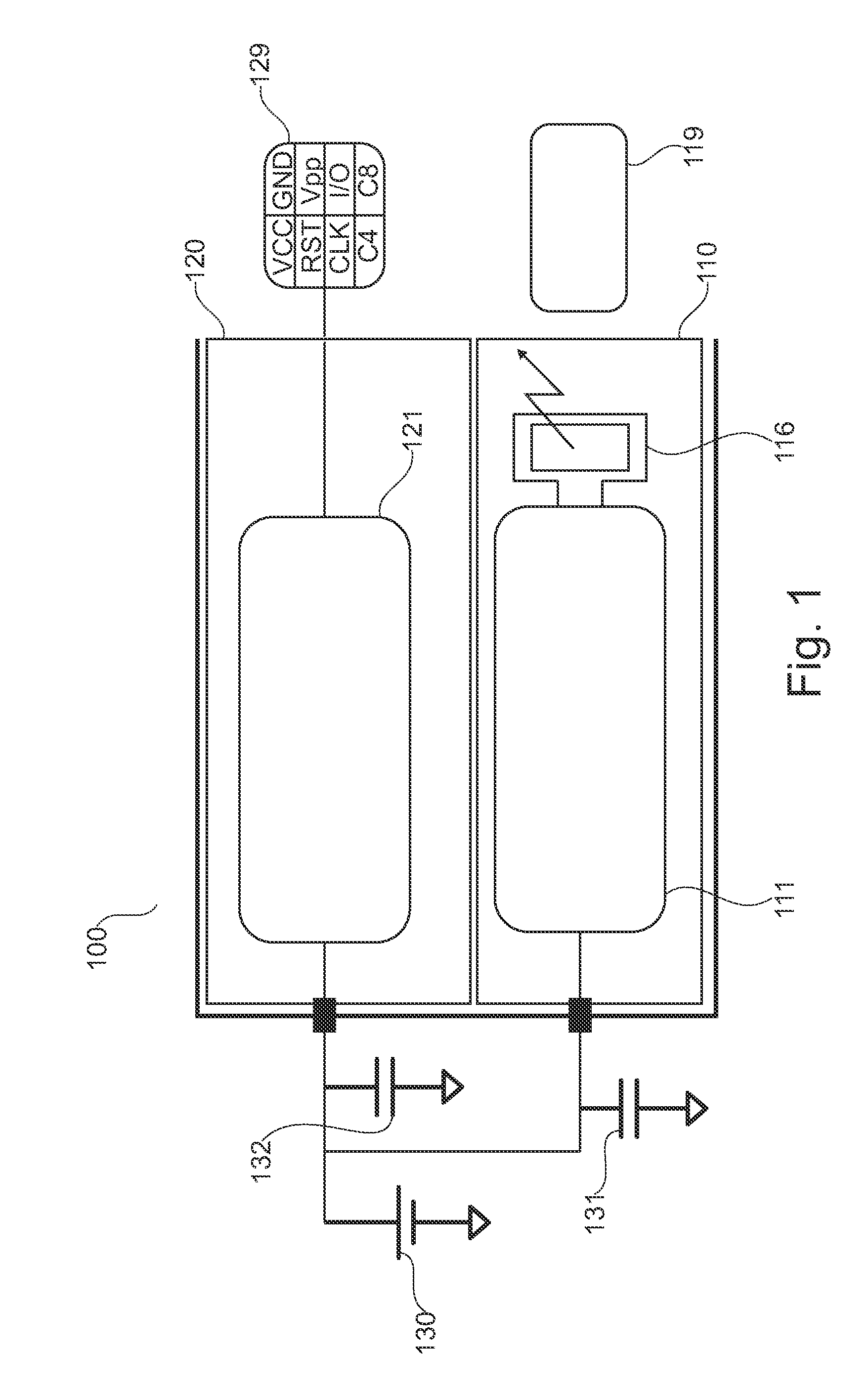
[0037]FIG. 1 is a block diagram showing the general structure of an electronic device 100 in accordance with an embodiment. More specifically, the electronic device 100 comprises a first circuit 110 and a second circuit 120 on a single chip. The first circuit 110 comprises an NFC contactless frontend 111 and antenna 116 for communicating with an NFC contactless card 119. The second circuit 120 comprises a contact frontend 121 for communicating with a contact card 129. Both the first circuit 110 and the second circuit 120 are connected to a common power supply 130, such as a battery or any other type of power supply and have respective input decoupling capacitances 131 and 132. To assure correct operation of the circuits 110 and 120, some kind of voltage reg...


PUM

PropertyMeasurementUnit
Frequencyaaaaaaaaaa
Frequencyaaaaaaaaaa
Electric potential / voltageaaaaaaaaaa

Abstract

There is described an electronic device, the device comprising (a) a power supply terminal for connecting to a power supply (130, 330), (b) a first circuit (110, 310) coupled to be powered by the power supply, the first circuit (110, 310) being susceptible to power supply noise within a predetermined frequency range, and (c) a second circuit (120, 320) coupled to be powered by the power supply, the second circuit (120, 320) comprising an open-loop capacitive DC-DC converter (323) having a switching frequency outside of the predetermined frequency range. There is also described a system comprising an electronic device and a reader/writer device. Furthermore, there is described a method of manufacturing an electronic device.

Description

CROSS-REFERENCE TO RELATED APPLICATIONS[0001]This application claims the priority under 35 U.S.C. §119 of European patent application no. 14156424.5, filed on Feb. 24, 2014, the contents of which are incorporated by reference herein.FIELD OF THE INVENTION[0002]The present invention relates to the field of electronic devices, in particular to integrated electronic devices comprising multiple circuits and a common power supply.ART BACKGROUND[0003]Several integrated electronic devices exist, in which two or more circuits are built on a single chip and supplied by a single, i.e. common power supply. In some cases, ripple (or other input noise) caused by one of the circuits may have a negative impact on the operation of another circuit. This problem occurs e.g. when an NFC contactless frontend is implemented on the same chip as a contact-card frontend and both frontends are to be supplied by a single battery. More specifically, a contact-card frontend usually includes a capacitive boost ...

Claims


Application Information

Patent Timeline
IPC IPC(8): H02M3/04H02M1/00
CPCH02M1/00H02M3/04H02M1/14H02M3/07Y10T29/49117
Inventor DALWADI, JAYDEEPEVANI, VENKATA SATYA SAI
Owner NXP BV
Why Eureka
Try Eureka