
Using High Resolution Full Die Image Data for Inspection

Active Publication Date: 2015-11-12
KLA TENCOR CORP
View PDF0 Cites 89 Cited by
  • Summary
  • Abstract
  • Description
  • Claims
  • Application Information

AI Technical Summary

Benefits of technology

This patent describes a method and system for determining the position of inspection data with respect to a stored high resolution die image. This can be used in the manufacturing process of wafers to help improve accuracy and efficiency. The method involves aligning data acquired by an inspection system with predetermined alignment sites in the die image space and determining the positions of these sites and the inspection data through a computer system. The system includes a storage medium with the stored high resolution die image and a processor for performing the method. Overall, this invention allows for more precise and automated inspection of wafers during manufacturing.

Problems solved by technology

However, in many circumstances, the design information may not be readily available.
In many instances, this data is either incomplete or unknown.

Method used


Image

  • Using High Resolution Full Die Image Data for Inspection
  • Using High Resolution Full Die Image Data for Inspection

Examples


Embodiment Construction

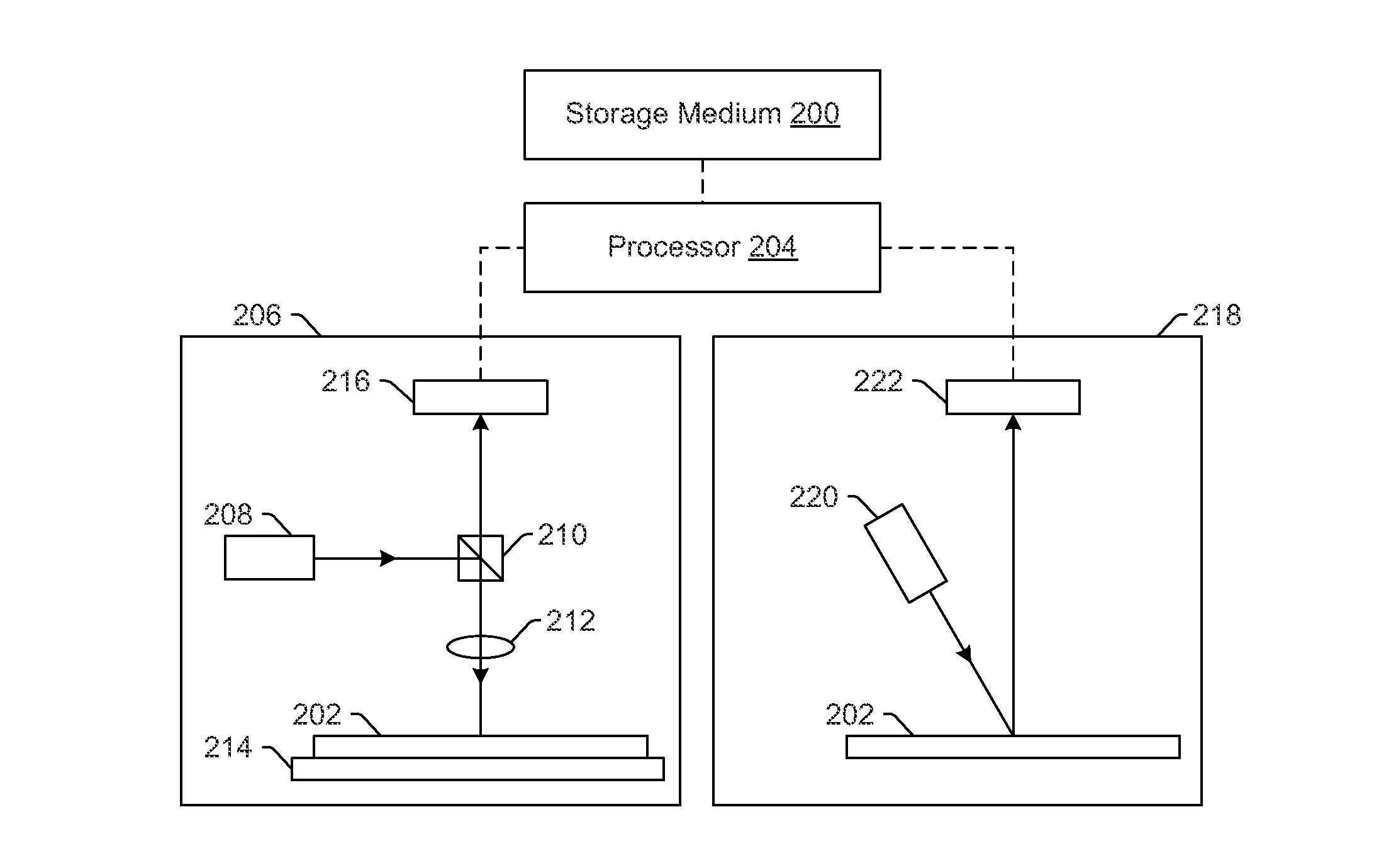
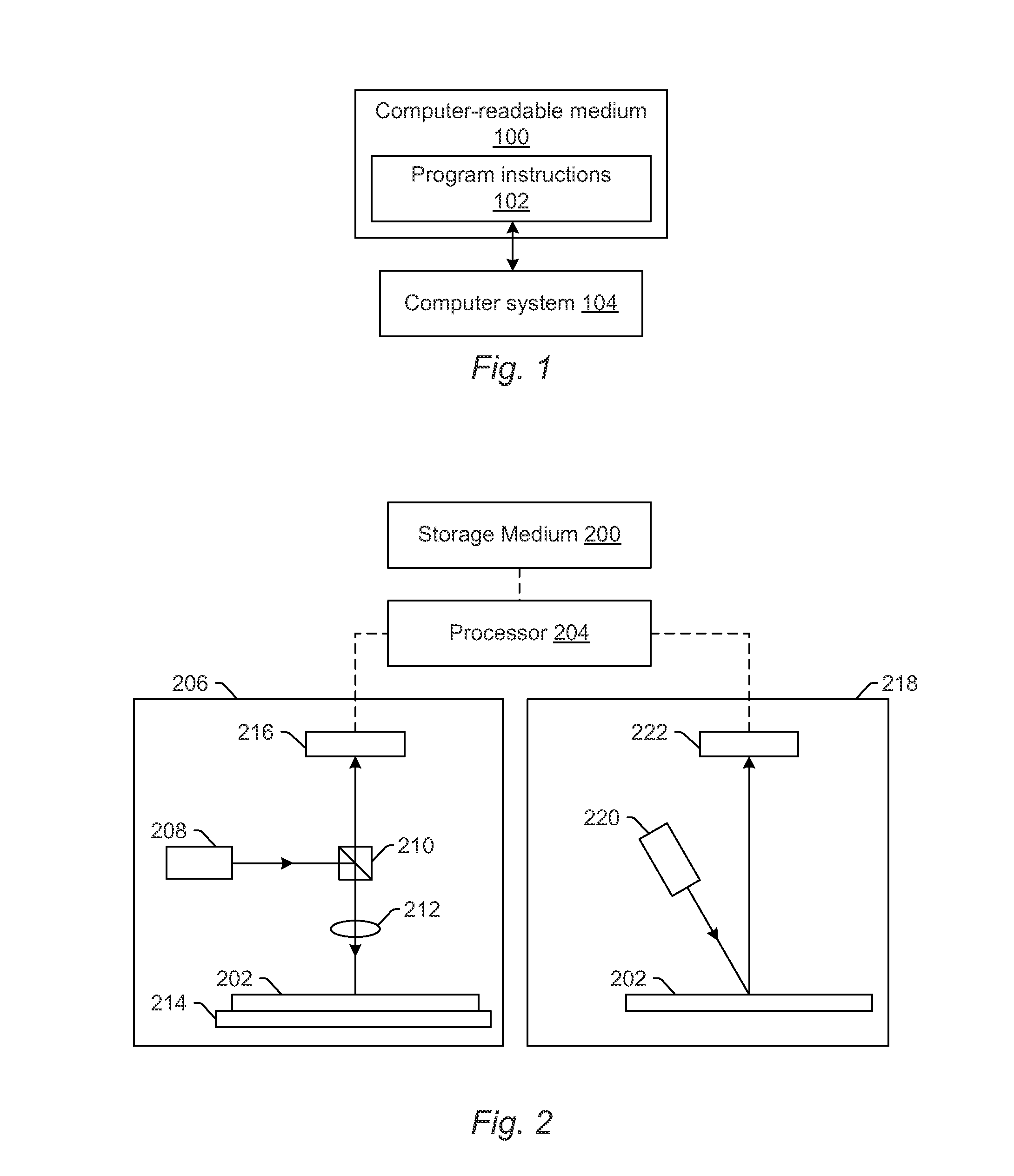
[0019]Turning now to the drawings, it is noted that the figures are not drawn to scale. In particular, the scale of some of the elements of the figures is greatly exaggerated to emphasize characteristics of the elements. It is also noted that the figures are not drawn to the same scale. Elements shown in more than one figure that may be similarly configured have been indicated using the same reference numerals. Unless otherwise noted herein, any of the elements described and shown may include any suitable commercially available elements.

[0020]In general, the embodiments described herein relate to methods and systems for utilizing high resolution full die image data in combination with inspection data. For example, one embodiment relates to a computer-implemented method for determining a position of inspection data with respect to a stored high resolution die image. The method includes aligning data acquired by an inspection system for alignment sites on a wafer with data for predete...


PUM


Abstract

Methods and systems for determining a position of inspection data with respect to a stored high resolution die image are provided. One method includes aligning data acquired by an inspection system for alignment sites on a wafer with data for predetermined alignment sites. The predetermined alignment sites have a predetermined position in die image space of a stored high resolution die image for the wafer. The method also includes determining positions of the alignment sites in the die image space based on the predetermined positions of the predetermined alignment sites in the die image space. In addition, the method includes determining a position of inspection data acquired for the wafer by the inspection system in the die image space based on the positions of the alignment sites in the die image space.

Description

BACKGROUND OF THE INVENTION[0001]1. Field of the Invention[0002]This invention generally relates to methods and systems for determining a position of inspection data with respect to a stored high resolution die image.[0003]2. Description of the Related Art[0004]The following description and examples are not admitted to be prior art by virtue of their inclusion in this section.[0005]Semiconductor manufacturing involves a large and complex set of imaging, etching, deposition and planarization processes in order to construct sub-micron (down to a few tens of nanometers) geometrical patterns on a silicon substrate. After a process has been performed to at least partially construct the patterns on the silicon substrate, the substrate must be inspected to determine if there are defects in the patterns or on the substrate. There are a number of different methods and systems that are used to inspect such substrates for defects. The type of method or system that is used for any particular su...

Claims


Application Information

Patent Timeline
IPC IPC(8): G06T7/00G06F17/50H01L21/67G01B21/16H01L21/66G06T7/60G01N21/88
CPCG06T7/001G06T7/60G06T7/0044G06F17/5045G01N21/8851G01N2201/12H01L22/12H01L21/67288G06T2207/30148G01N2201/10G01B21/16G01N21/8806G01N21/9501G01N2021/8825G01N2021/8887G01N23/2251G01N2223/6116G06T7/74G01N21/88G06F30/30
Inventor KULKARNI, ASHOK V.
Owner KLA TENCOR CORP
Features
  • Generate Ideas
  • Intellectual Property
  • Life Sciences
  • Materials
  • Tech Scout
  • Unparalleled Data Quality
  • Higher Quality Content
  • 60% Fewer Hallucinations
Learn More