

Display Device and Method of Manufacturing Thin Film Transistor
- Summary
- Abstract
- Description
- Claims
- Application Information
AI Technical Summary
Benefits of technology
Problems solved by technology
Method used
Image

Examples
first embodiment
The First Embodiment
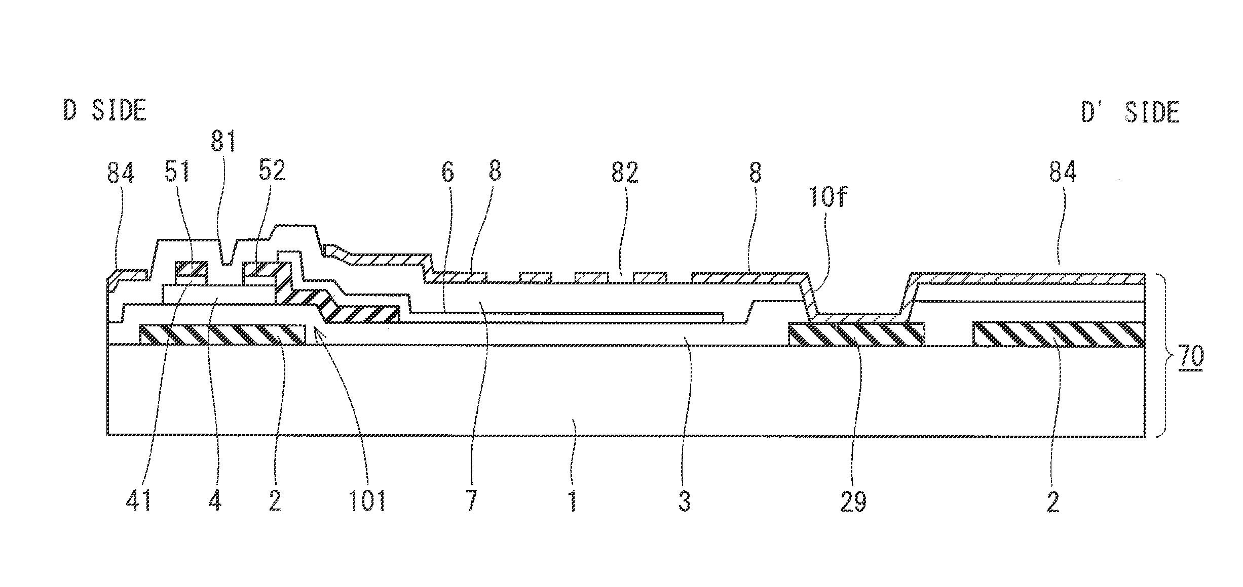
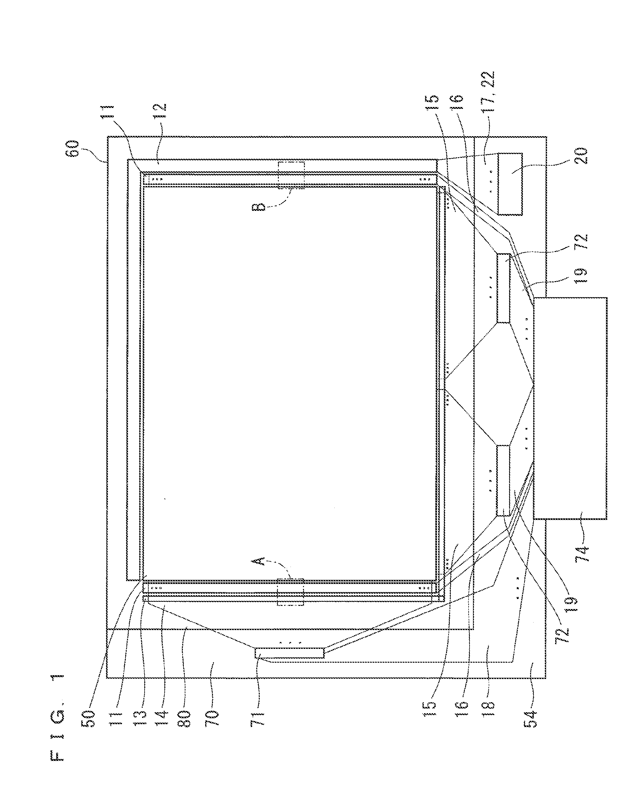
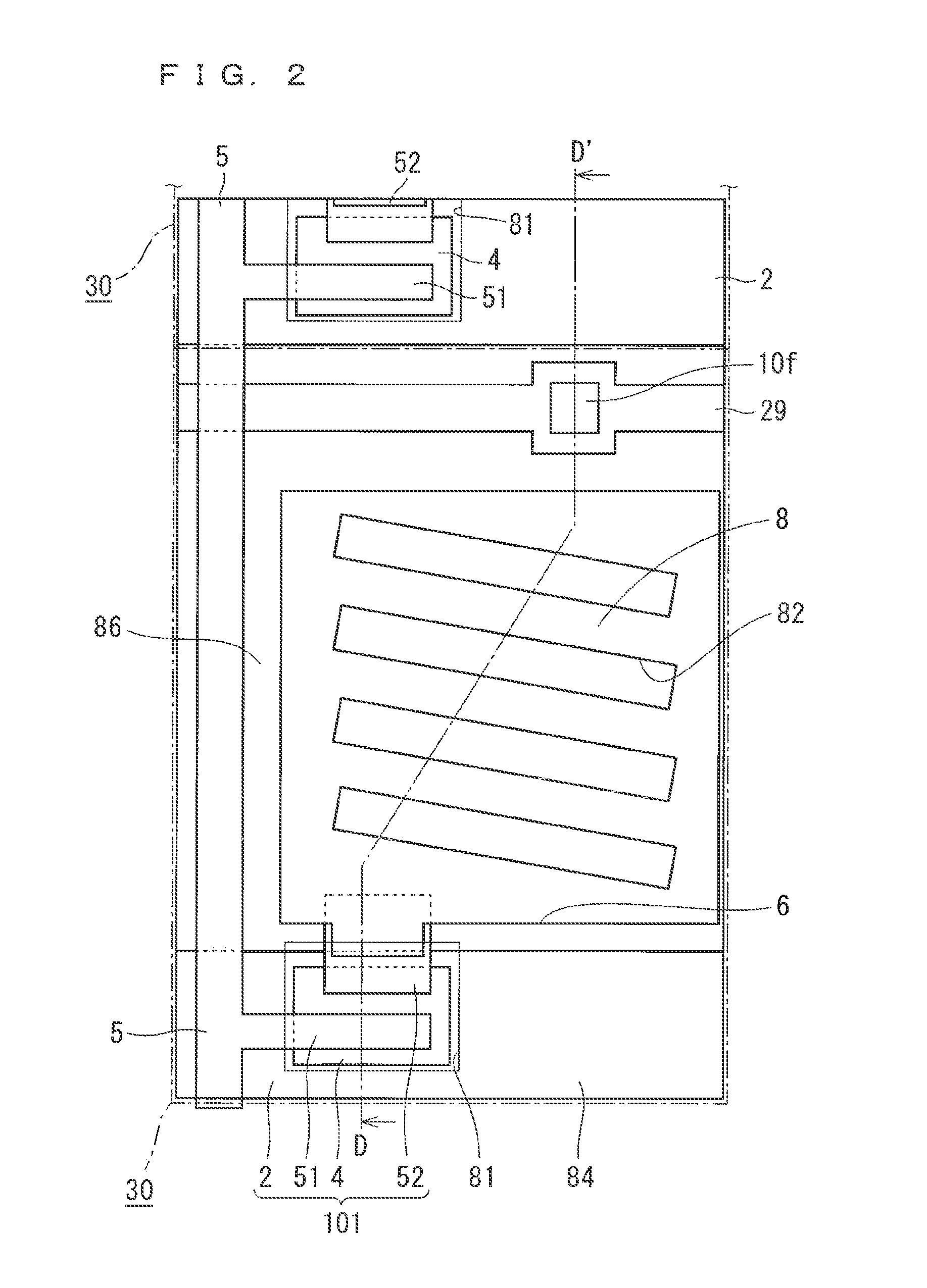
[0035]FIG. 1 is a plan view schematically showing a structure of a FFS liquid crystal display in accordance with the first embodiment.
[0036]The liquid crystal display has a liquid crystal display panel 60. The liquid crystal display panel 60 comprises an array substrate 70 and a counter substrate 80 facing the array substrate 70 in a plan-view direction.
[0037]The array substrate 70 is divided into a display area 50 and a frame area 54 on an outer side of the display area 50 in a plan view.
[0038]The array substrate 70 and the counter substrate 80 are attached to each other with a sealing material (not shown), to constitute the liquid crystal display panel 60. More specifically, the array substrate 70 and the counter substrate 80 each have an orientation film, and these orientation films are stacked on each other in a facing manner. These substrates are provided with a gap of about several μm formed by a spacer material formed of an organic resin or the like and at...
second embodiment
The Second Embodiment
[0140]In the second embodiment of the present invention, a preferred method of forming the wire 53 and the electrode 55, and the source electrode 51 and the drain electrode 52 in the same process will be described. More specifically, a photomask used for forming the contact hole 9a or 9b is made common to a photomask used for forming the semiconductor film 4.
[0141]The structure obtained by the manufacturing method described in the second embodiment is the same as that shown in the first embodiment, and therefore the second embodiment produces the same effect as that of the first embodiment, for increasing display quality without widening the frame area.
[0142]FIGS. 9 to 16 are cross sections used for explanation of a flow of manufacturing process of a display device in accordance with the second embodiment. In these figures, on the left side of the break line, shown is a cross section of an area where the TFT 101 (see FIGS. 1 and 3) is to be formed, and on the ri...
PUM
 Abstract
Description
Claims
Application Information