
Automatic Recipe Stability Monitoring and Reporting

a technology of automatic recipe and stability monitoring, applied in the direction of total factory control, programme control, instruments, etc., can solve the problems of inspection recipe no longer suitable for inspection of the type of wafer, inspection of a wafer on one tool may not be suitable for inspection of the same wafer on another tool, inspection of a wafer on one tool may not be suitable for inspection of different wafers on the same tool,

Active Publication Date: 2015-12-17
KLA TENCOR TECH CORP
View PDF20 Cites 7 Cited by
  • Summary
  • Abstract
  • Description
  • Claims
  • Application Information

AI Technical Summary

Benefits of technology

The patent describes a method and system for monitoring the stability of a wafer inspection recipe over time. This helps to ensure consistent and accurate results from inspecting wafers at different points in time. The method involves collecting inspection results, identifying abnormal variations in the results, and determining if the variation is caused by the wafers, the recipe, or the inspection tools. This can be performed by a computer system and helps to maintain the reliability and effectiveness of the inspection process.

Problems solved by technology

However, as the dimensions of semiconductor devices decrease, inspection becomes even more important to the successful manufacture of acceptable semiconductor devices because smaller defects can cause the devices to fail.
For example, one inspection recipe that is suitable for inspection of a wafer on one tool may not be suitable for inspection of the same wafer on another tool.
In addition, one inspection recipe that is suitable for inspection of a wafer on one tool may not be suitable for inspection of different wafers on the same tool.
Once an inspection recipe has been set up, there are certain circumstances that can cause that inspection recipe to be no longer suitable for inspection of the type of wafers and tool that it was setup for.
For instance, a change in one or more fabrication processes performed on the wafers, which an inspection recipe was setup for, may cause that inspection recipe to detect an abnormal number of defects on the wafers, which may not even be defects if the change in the one or more fabrication processes do not cause the wafers to be defective.
In addition, if there are certain changes in the inspection tool itself (e.g., due to drift in one or more properties of one or more optical elements of the inspection tool), the changes in the inspection tool can cause an inspection recipe to be no longer suitable for inspection of the wafers the recipe was setup for.
Until it can be determined that the inspection results reflect defects on the wafer rather than drifts in the process used to fabricate the wafer or the inspection tool itself, those inspection results are not only useless but acting on those inspection results (e.g., changing the fabrication process) can actually cause real defects on wafers (e.g., if a perfectly fine fabrication process is altered to reduce “defects” detected on a wafer that are not defects at all but are detected as such due to drifts in the inspection tool).
Separating out influences on the inspection results can be a particularly difficult challenge.
For instance, an abnormal number of defects detected on a wafer may be an abnormal number of actual defects on the wafer caused by a fabrication process failure.
However, the abnormal number of defects may be caused by acceptable drifts in the fabrication process and / or unacceptable changes in the inspection tool.
Currently, however, there is no known utility to periodically monitor the stability of inspection recipes for specific layers of semiconductor wafers that are inspected on multiple optical inspection tools used in a production time.
Without the ability to monitor inspection results such as image patches and statistics collected from them for a given semiconductor wafer layer, it is very difficult to manually identify when a certain recipe becomes invalid for the inspection of the respective layer, due to variations in a semiconductor process.

Method used


Image

  • Automatic Recipe Stability Monitoring and Reporting
  • Automatic Recipe Stability Monitoring and Reporting
  • Automatic Recipe Stability Monitoring and Reporting

Examples


Embodiment Construction

[0025]Turning now to the drawings, it is noted that the figures are not drawn to scale. In particular, the scale of some of the elements of the figures is greatly exaggerated to emphasize characteristics of the elements. It is also noted that the figures are not drawn to the same scale. Elements shown in more than one figure that may be similarly configured have been indicated using the same reference numerals. Unless otherwise noted herein, any of the elements described and shown may include any suitable commercially available elements.

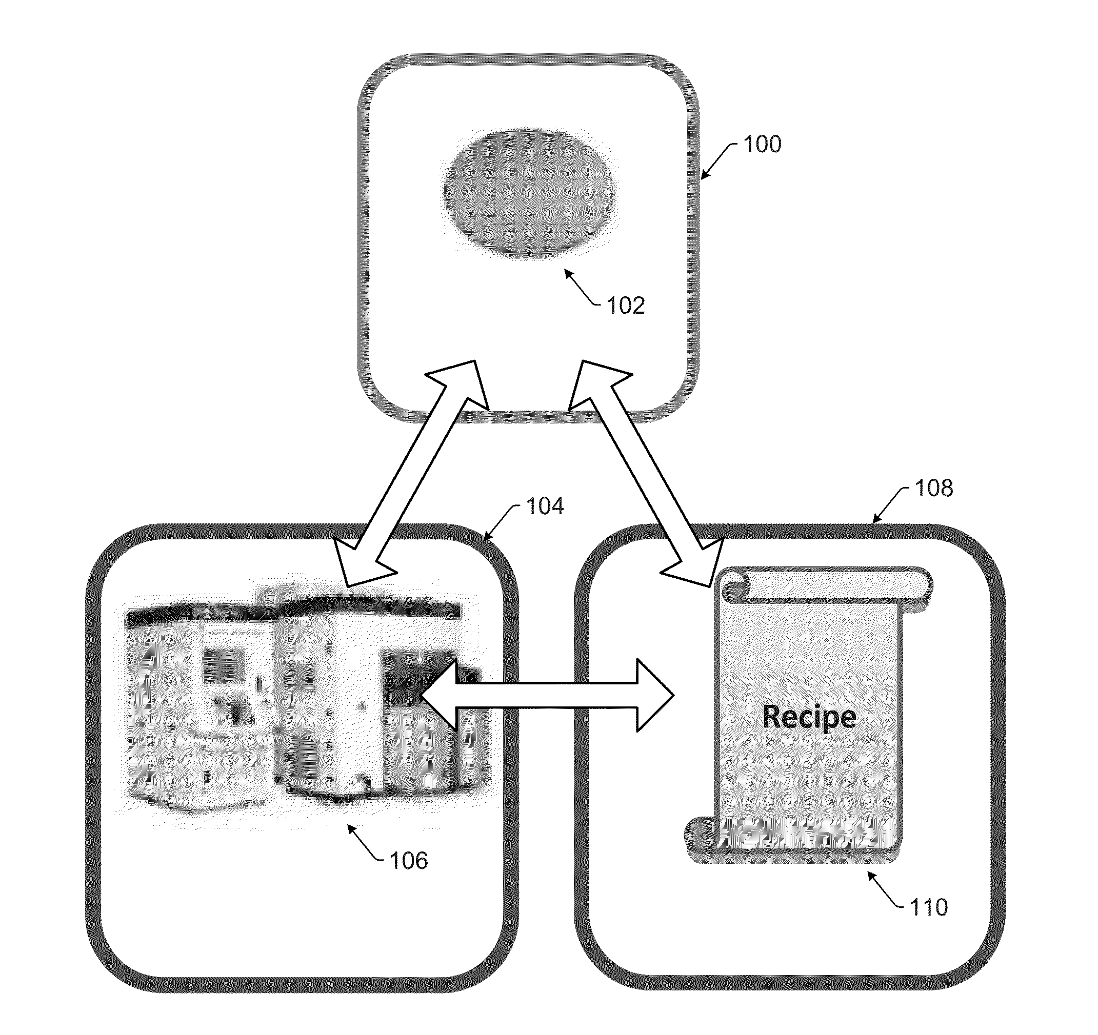
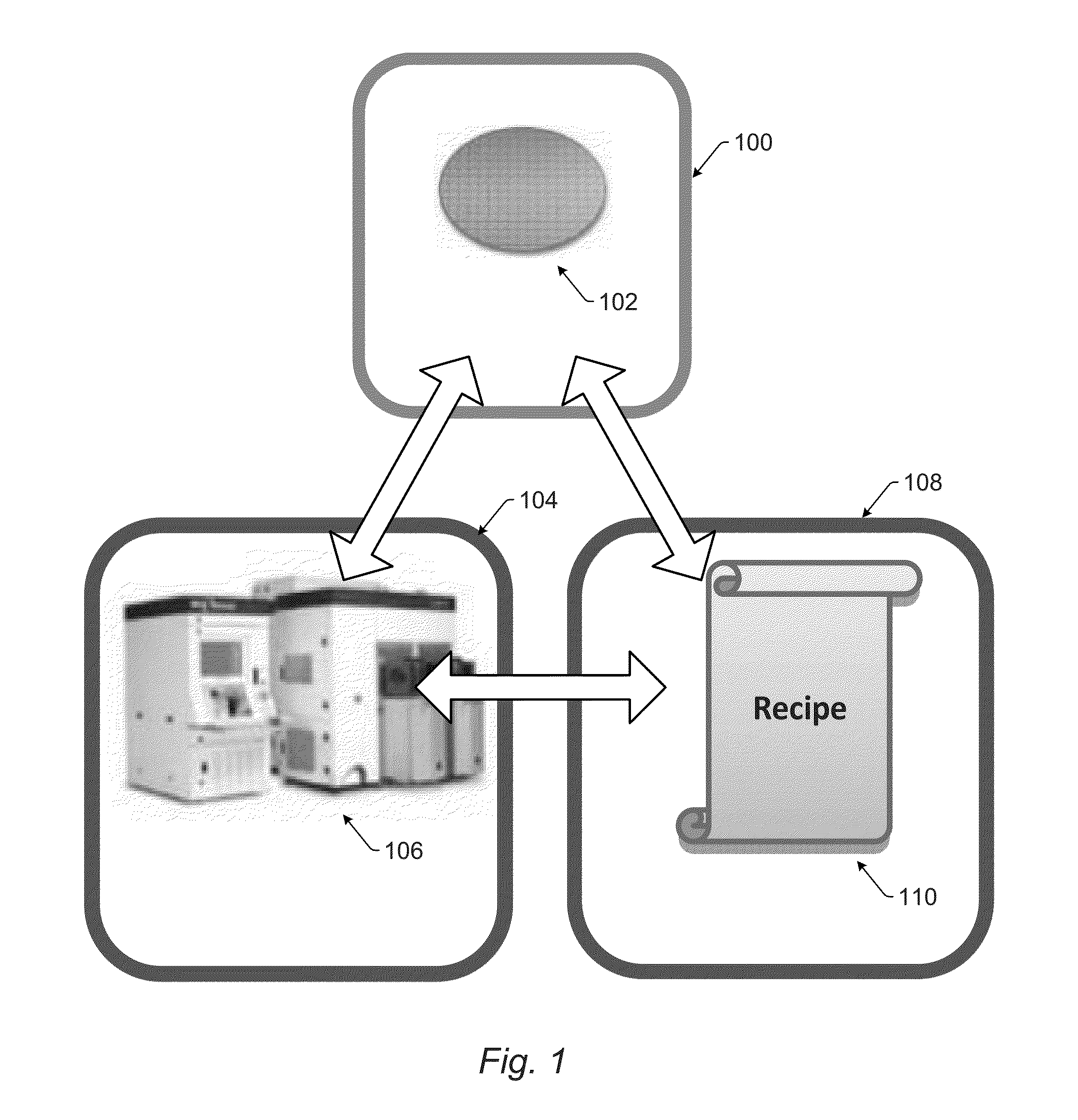
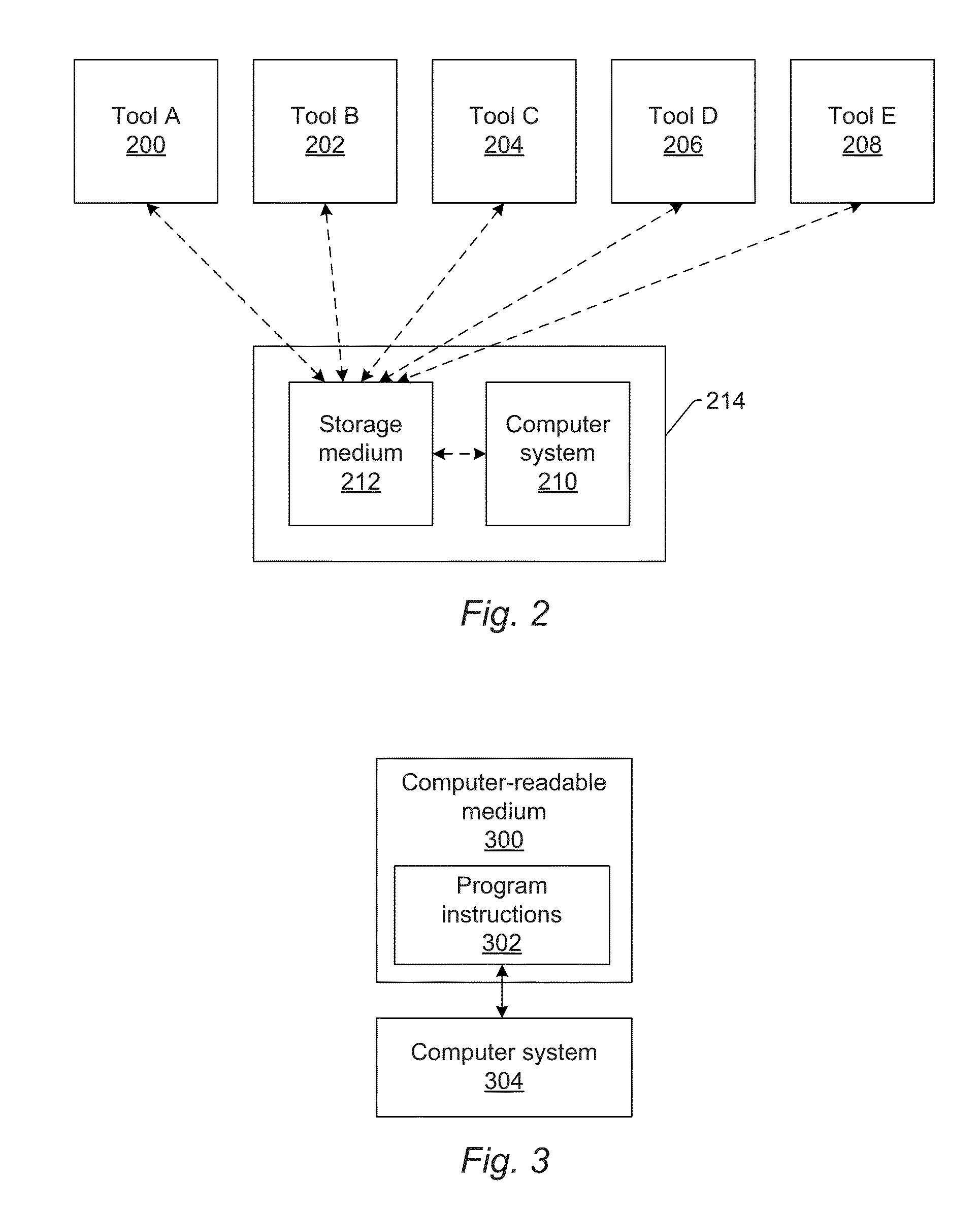
[0026]The embodiments described herein generally relate to automatic recipe stability monitoring and reporting. One embodiment relates to a computer-implemented method for monitoring stability of a wafer inspection recipe over time. The embodiments described herein provide an approach to automatically compute and monitor important metrics related to stability of inspection recipes on production inspection tools, based on information collected from wa...


PUM


Abstract

Systems and methods for monitoring stability of a wafer inspection recipe over time are provided. One method includes collecting inspection results over time. The inspection results are generated by at least one wafer inspection tool while performing the wafer inspection recipe on wafers at different points in time. The method also includes identifying abnormal variation in the inspection results by comparing the inspection results generated at different times to each other. In addition, the method includes determining if the abnormal variation is attributable to the wafers, the wafer inspection recipe, or one or more of the at least one wafer inspection tool thereby determining if the wafer inspection recipe is stable over time.

Description

BACKGROUND OF THE INVENTION[0001]1. Field of the Invention[0002]The present invention generally relates to systems and methods for automatic recipe stability monitoring and reporting.[0003]2. Description of the Related Art[0004]The following description and examples are not admitted to be prior an by virtue of their inclusion in this section.[0005]Inspection processes are used at various steps during a semiconductor manufacturing process to detect defects on wafers to promote higher yield in the manufacturing process and thus higher profits. Inspection has always been an important part of fabricating semiconductor devices such as ICs. However, as the dimensions of semiconductor devices decrease, inspection becomes even more important to the successful manufacture of acceptable semiconductor devices because smaller defects can cause the devices to fail.[0006]Inspection processes are usually performed on inspection tools by executing a set of instructions, normally called a “recipe,” ...

Claims


Application Information

Patent Timeline
IPC IPC(8): G05B19/401G05B19/406
CPCG05B19/401G05B2219/37224G05B19/406G05B19/41875G05B2219/32196G05B2219/32222Y02P90/02
Inventor LEE, HUCHENGGAO, LISHENGTHATTAISUNDARAM, GOVINDARAJAN
Owner KLA TENCOR TECH CORP
Learn More