Pixel structure of display panel
- Summary
- Abstract
- Description
- Claims
- Application Information
AI Technical Summary
Benefits of technology
Problems solved by technology
Method used
Image

Examples
Embodiment Construction
[0044]To provide a better understanding of the present invention to the skilled users in the technology of the present invention, preferred embodiments will be detailed as follows. The preferred embodiments of the present invention are illustrated in the accompanying drawings with numbered elements to elaborate the contents and effects to be achieved.
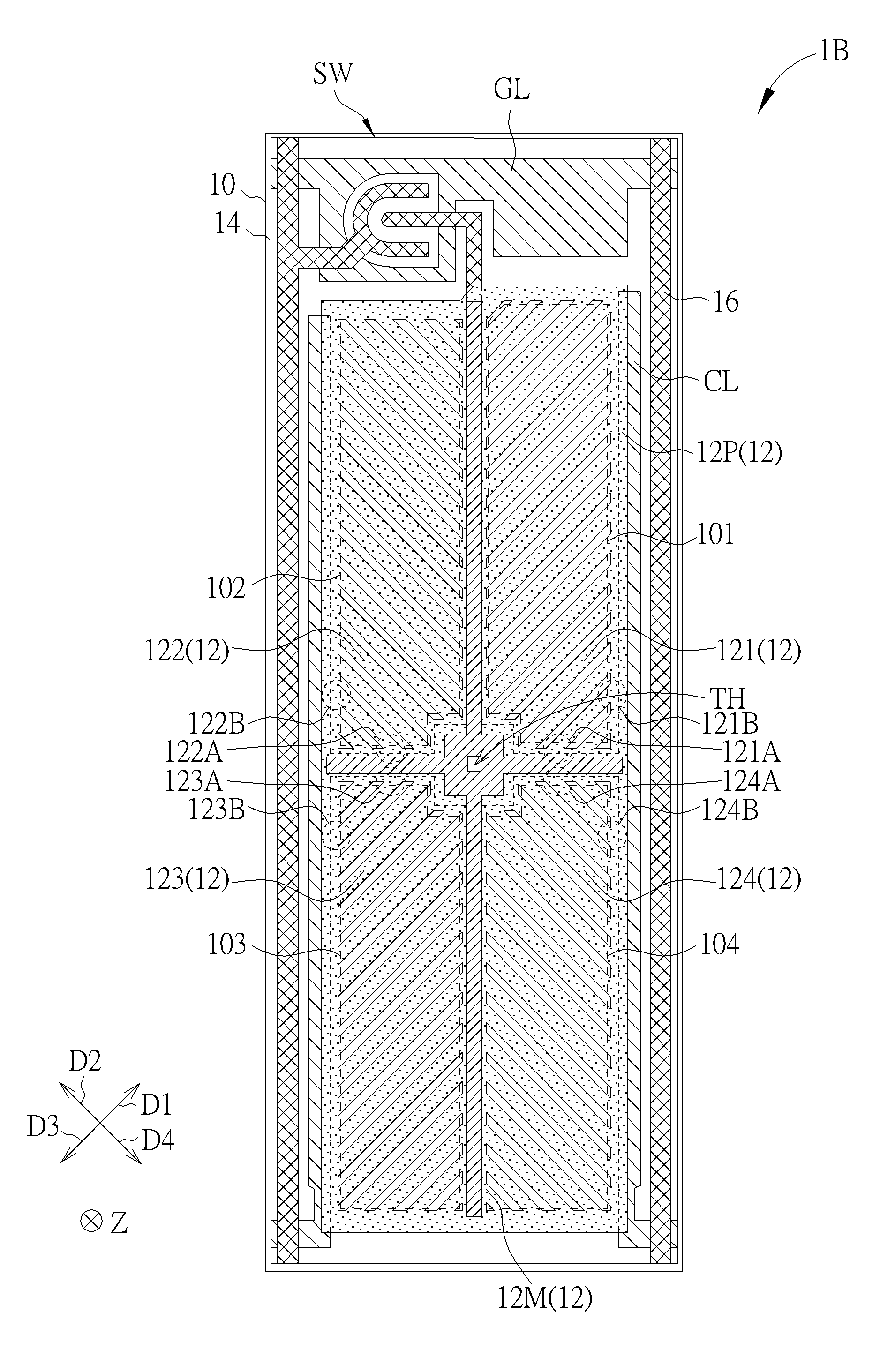
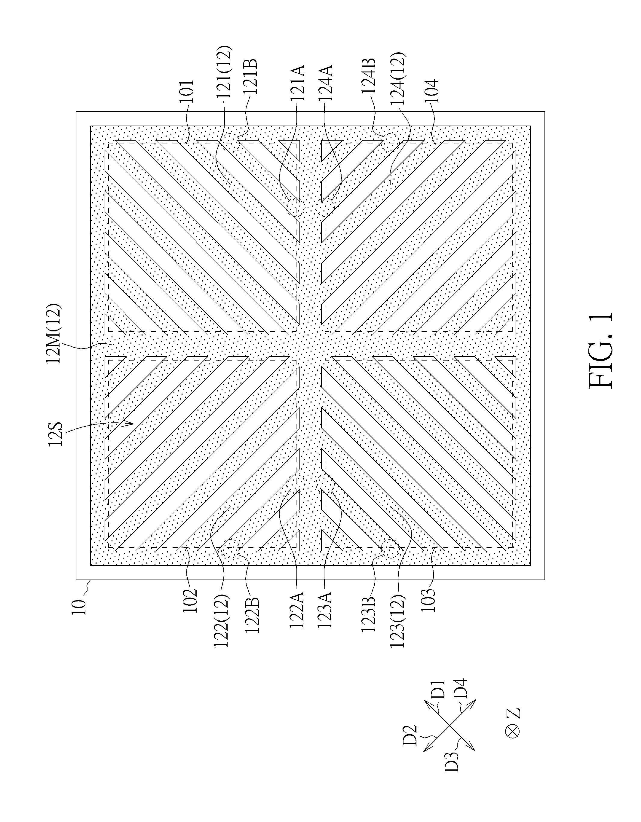
[0045]Please refer to FIGS. 1-5. FIG. 1 is a top view schematically illustrating a first pixel electrode of a pixel structure of display panel according to a first embodiment of the present invention, FIG. 2 is a top view schematically illustrating an insulation layer of the pixel structure of display panel according to the first embodiment of the present invention, FIG. 3 is a top view schematically illustrating a second pixel electrode of the pixel structure of display panel according to the first embodiment of the present invention, FIG. 4 is a top view schematically illustrating the pixel structure of display panel when not driven b...
PUM
| Property | Measurement | Unit |
|---|---|---|
| Electric potential / voltage | aaaaa | aaaaa |
Abstract
Description
Claims
Application Information
 - Generate Ideas
- Intellectual Property
- Life Sciences
- Materials
- Tech Scout
- Unparalleled Data Quality
- Higher Quality Content
- 60% Fewer Hallucinations
Browse by: Latest US Patents, China's latest patents, Technical Efficacy Thesaurus, Application Domain, Technology Topic, Popular Technical Reports.
© 2025 PatSnap. All rights reserved.Legal|Privacy policy|Modern Slavery Act Transparency Statement|Sitemap|About US| Contact US: help@patsnap.com