Semiconductor device

Active Publication Date: 2016-02-04
MITSUBISHI ELECTRIC CORP
View PDF3 Cites 0 Cited by
  • Summary
  • Abstract
  • Description
  • Claims
  • Application Information

AI Technical Summary

Benefits of technology

The patent text explains how to easily create semiconductor devices that can be connected to external elements. This makes it simple to create the entire circuitry needed for the device.

Problems solved by technology

Consequently, the substrate pattern wiring for the entire circuitry including such semiconductor device is limited.
Thus, the substrate has unfortunately been difficult to design flexibly.

Method used


Image

  • Semiconductor device
  • Semiconductor device
  • Semiconductor device

Examples


first preferred embodiment

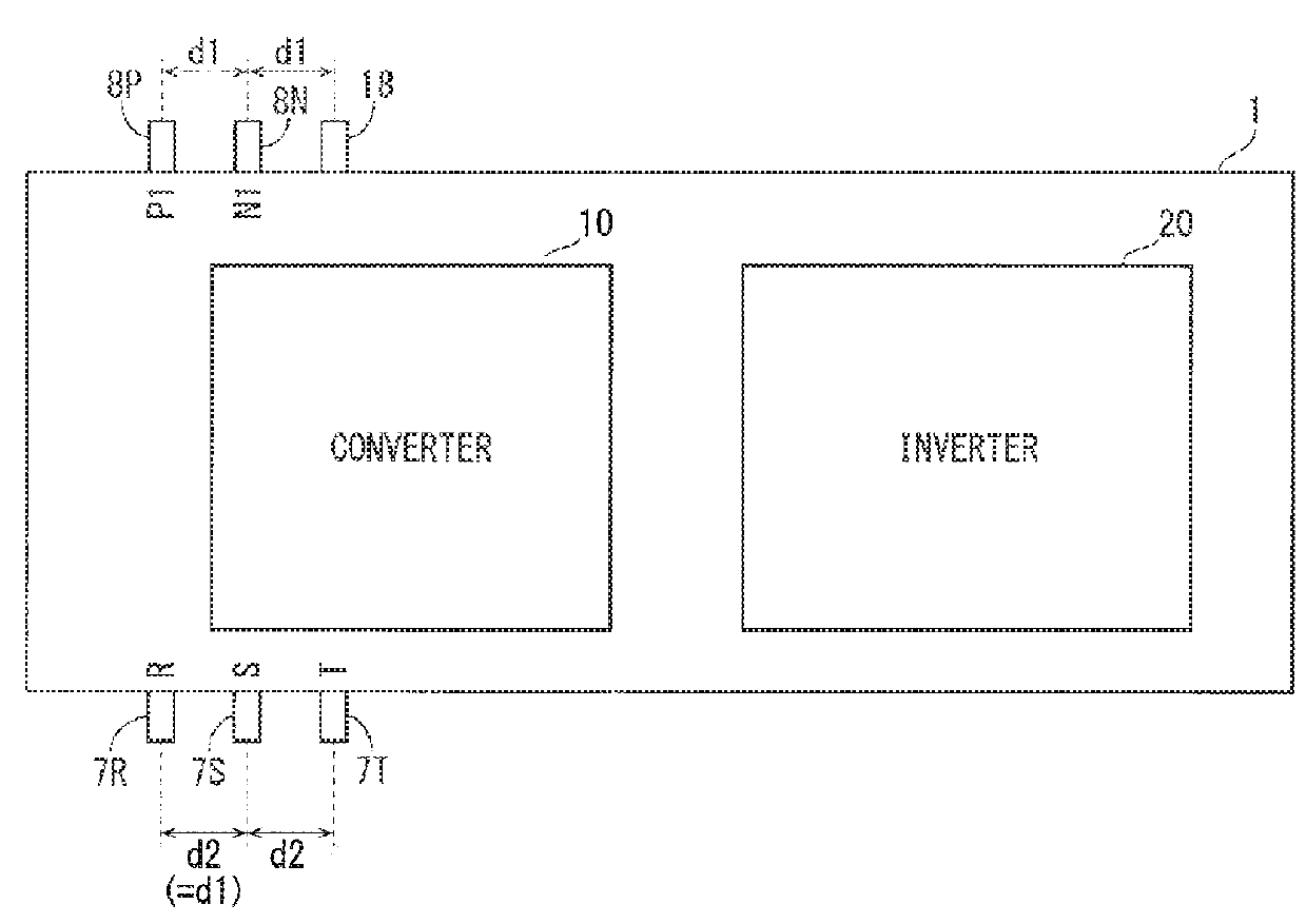
[0022]FIG. 1 is a diagram describing a configuration of a composite module 1 according to a first preferred embodiment of the present invention. The composite module 1 according to the first preferred embodiment is a semiconductor device that has a rectangular shape in plan view and integrally includes a converter 10 and an inverter 20 in a sealing resin.

[0023]As shown in FIG. 1, converter output terminals 8P and 8N (P1 and N1) for external connection of the converter 10 are located adjacent to each other on a first side (the upper part in FIG. 1). An external terminal 18 (adjacent external terminal) for external connection of the composite module 1 is located adjacent to the converter output terminal 8N. The external terminal 18 may be provided for the converter 10, for the inverter 20, or for both the converter 10 and the inverter 20.

[0024]AC input terminals 7R, 7S, and 7T (R, S, and T) that are the converter input terminals for external connection of the converter 10 are located ...

second preferred embodiment

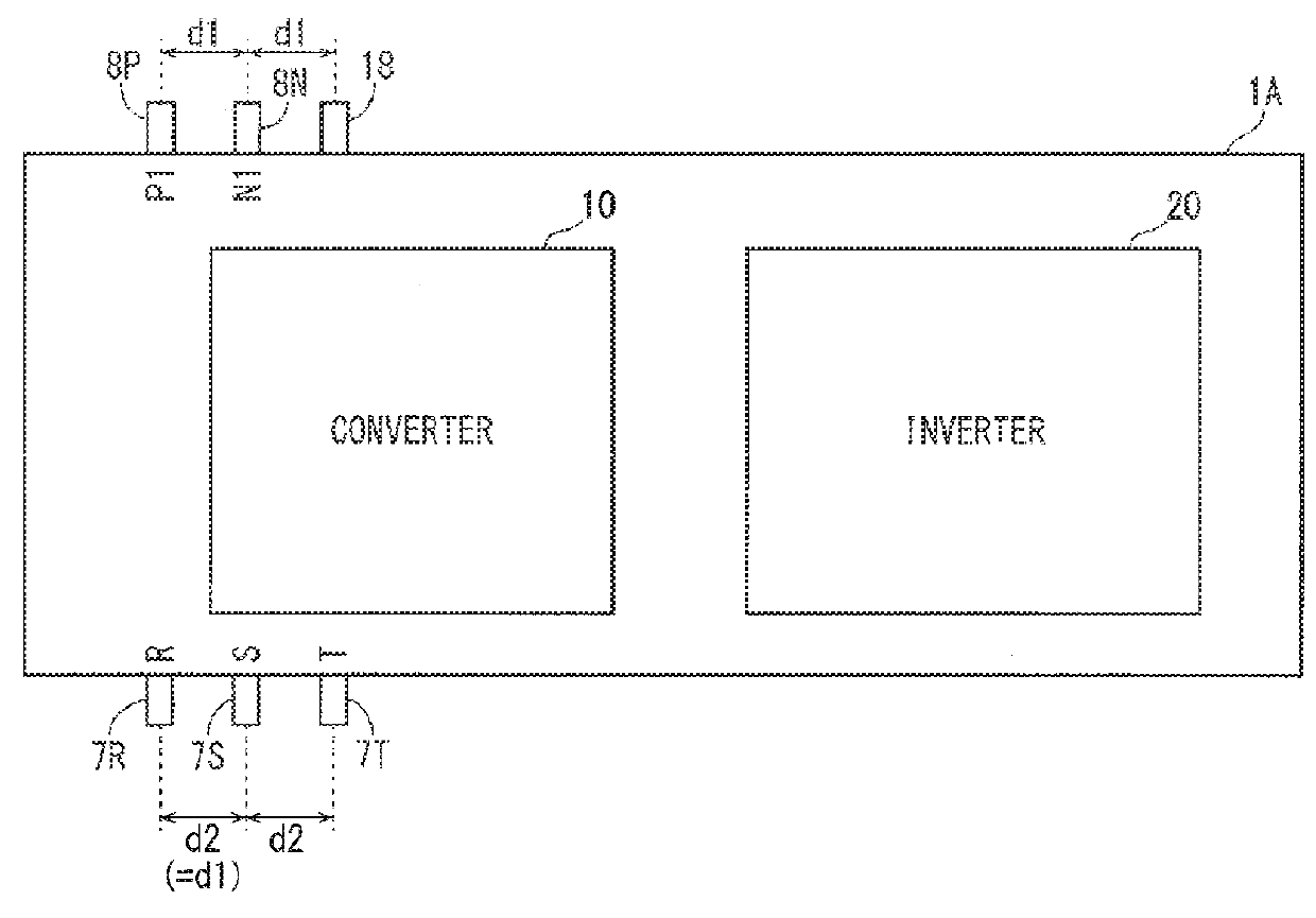
[0033]FIG. 4 is a diagram describing a configuration of a composite module 2 according to a second preferred embodiment of the present invention. As shown in FIG. 4, the composite module 2 integrally includes, in addition to the converter 10 and the inverter 20, a brake 30 embedded in the sealing resin. The configuration except for the brake 30 is similar to that of the composite module 1 according to the first preferred embodiment shown in FIGS. 1 to 3.

[0034]FIG. 5 is a circuit diagram illustrating equivalent circuits in the converter 10, the inverter 20, and the brake 30 shown in FIG. 4.

[0035]As shown in FIG. 5, the converter 10 includes diodes D1, D2, and D3 and diodes D4, D5, and D6 located between the converter output terminals 8P and 8N. More particularly, the cathodes of the respective diodes D1, D2, and D3 are connected in common to the converter output terminal 8P, the anodes of the diodes D1, D2, and D3 are electrically connected to the cathodes of the diodes D4, D5, and D...

third preferred embodiment

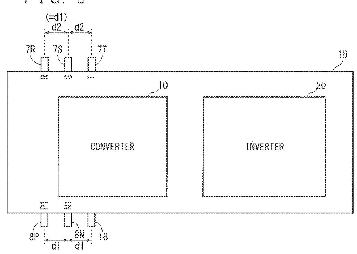
[0046]FIG. 6 is a diagram describing a configuration of a composite module 3 according to a third preferred embodiment of the present invention. As shown in FIG. 6, similarly to the composite module 2 according to the second preferred embodiment, the composite module 3 integrally includes, in addition to the converter 10 and the inverter 20, the brake 30 embedded in the sealing resin.

[0047]The composite module 3 includes, as the external terminal 18, the IGBT emitter terminal 9N that is electrically connected to the emitter of the IGBT 40. The IGBT emitter terminal 9N is located adjacent to the converter output terminal 8N on one main-surface side having the converter output terminals 8P and 8N provided thereon. The IGBT emitter terminal 9N is located, as the external terminal 18, at the formation pitch d1 away from the converter output terminal 8N, thereby being categorized as the first terminal group together with the converter output terminals 8P and 8N. The configuration except ...


PUM


Abstract

Converter output terminals of a converter are located adjacent to each other on a first side and an external terminal for external connection of a composite module is located adjacent to the converter output terminal. AC input terminals of the converter are located on a second side. Each of the distances between the converter output terminals and between the converter output terminal and the external terminal is set to a first formation pitch. Each of the distances between the AC input terminals is set to a second formation pitch. The first formation pitch is set to be equal to the second formation pitch.

Description

BACKGROUND OF THE INVENTION[0001]1. Field of the Invention[0002]The present invention relates to a semiconductor device having a modular structure in which a converter and an inverter are integrally included.[0003]2. Description of the Background Art[0004]As disclosed in, for example, International Publication No. WO 98 / 10508 (FIG. 15), a semiconductor device has a molecular structure described as follows. The semiconductor device includes a metal substrate, a plurality of wires that are fixed to the metal substrate with an insulating layer therebetween, and power circuitry that is electrically connected to the plurality of wires. The power circuitry includes a plurality of circuit portions (such as a converter circuit portion) that are electrically connected between the plurality of wires. The circuit portions include a plurality of external terminals for external connection that are integral therewith and are bonded to the plurality of wires.[0005]The traditional semiconductor dev...

Claims


Application Information

Patent Timeline
IPC IPC(8): H02M7/00H02M1/00H02M5/458H02M7/06H02M7/537
CPCH02M7/003H02M5/4585H02M7/06H02M7/537H01L2224/48139H01L2224/49111H01L2224/49113H05K7/14329H05K7/1432
Inventor YAMAGUCHI, KOSUKETANAKA, TOMOFUMINAKAGAWA, SHINYAIWAGAMI, TORU
Owner MITSUBISHI ELECTRIC CORP
Why Eureka
Try Eureka