[0116]Concerning
temperature control mechanisms,
temperature control of the
gate valve is an
advantage of the present invention for the following reasons. First, the portion of the gate valve exposed to the reactor chamber (equivalently, exposed face) is preferably maintained at a high enough temperature so that gases in the reactor do not condense on the exposed face and so that unwanted reactions or
complex formation are not induced in the gases in the reactor by contact with the exposed face. Second, the portions of the gate valve that physically oppose and form a seal with corresponding portions of the entrance
assembly of the reactor (equivalently, the sealing portion of the gate valve and the sealing portions of the reactor
assembly) are preferably maintained at a low enough temperature so that
thermal damage to auxiliary components of the unit, e.g., o-rings, seals, gaskets, etc, is limited or prevented. Also, the temperature of the exposed face should remain below the deposition / reaction temperatures, but this is virtually always the case.
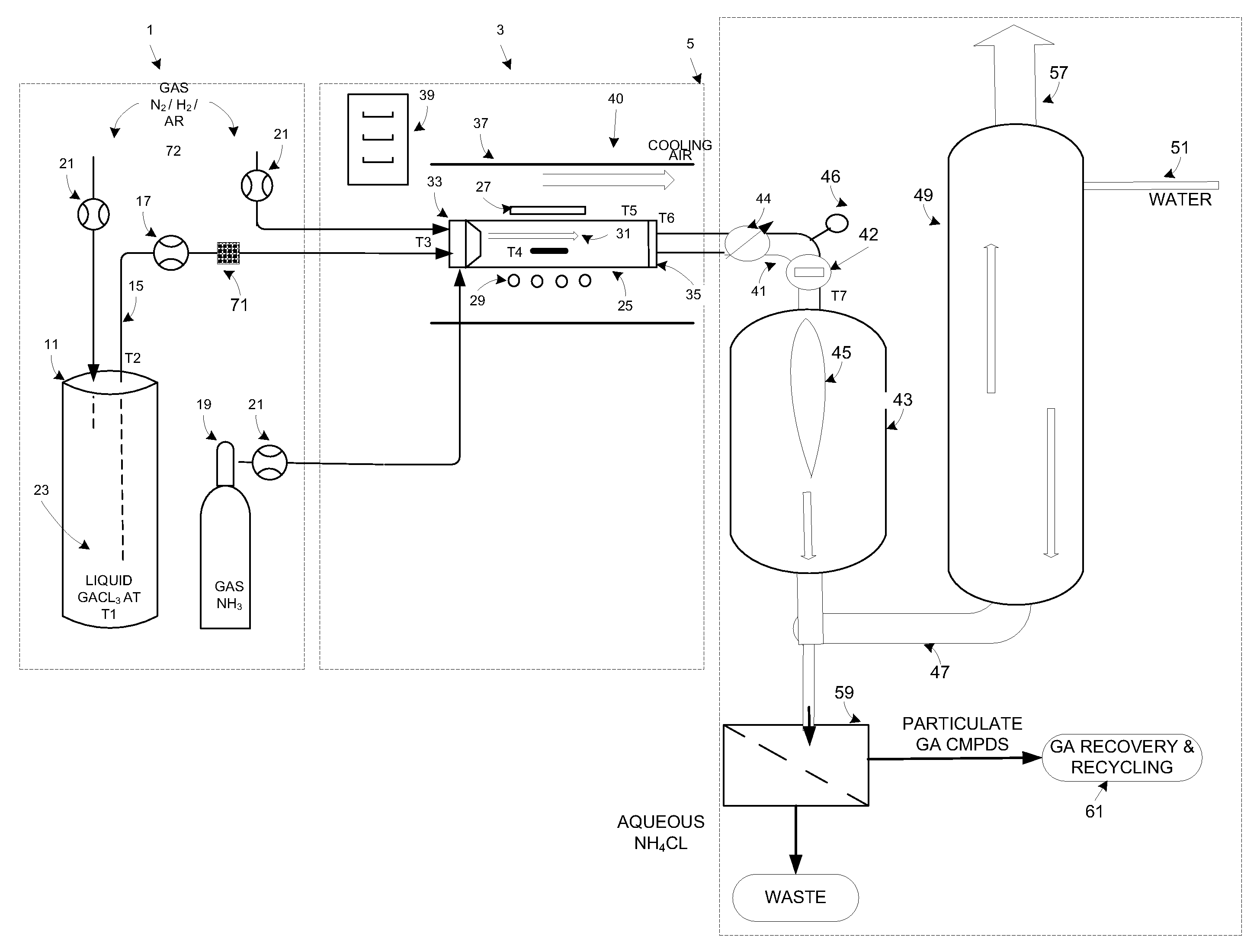
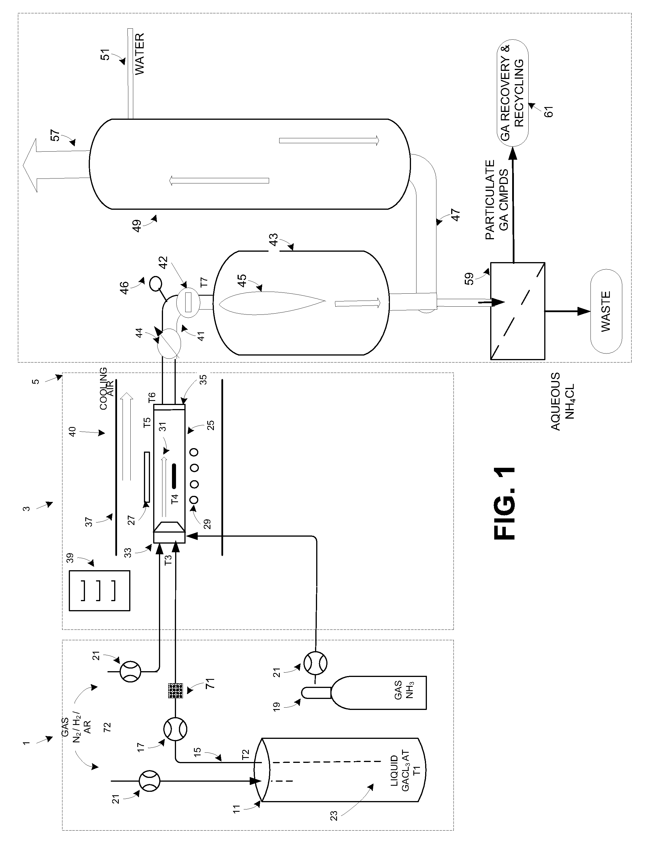
[0117]High and low temperature thresholds depend on the particular process being conducted in a reactor chamber. In the case of HVPE growth of GaN, significant temperature thresholds include: the
condensation temperature of reaction precursor GaCl3 at or below ≈80° C. into a liquid form; the
condensation temperature of
reaction product NH4Cl at or below ≈140-150° C. into a
solid form (i.e., the reverse of sublimation); and the safe operating temperatures of currently-available,
chlorine-resistant sealing materials at or below ≈150-160° C. (here, “≈” is a common mathematical symbol used herein with its common meaning of about or approximately).
[0118]Preferred gate valve assemblies (e.g., a combination of a gate valve and
temperature control mechanisms) comprise both mechanisms capable of raising the temperature of an exposed face of the gate valve and lowering the temperature of a sealing portion. Further embodiments, however, can comprise only a temperature raising mechanism, or a temperature lowering mechanism, or neither. Further embodiments can comprise multiple mechanisms of either type. Also, temperature control mechanisms can be integral to the gate valve, or integral (or closely adjacent) to the sealing portion of the reactor, or external to but associated with the gate valve or the reactor, or a combination of such arrangements. In the following, preferred, but non-limiting, temperature control mechanisms are described. However, the invention can include temperature mechanism other than those described.
[0119]The exposed face of a gate valve can be heated by conduction from the body of the gate valve, which in turn can be heated by a number temperature control devices known to those with ordinary skill in the art, including but not limited to, resistance heating,
induction heating,
radiant heating, high temperature gas / liquid heating etc. In one preferred embodiment, the body (and thereby also the exposed face) of the gate valve can be heated and controlled by
radiant heating elements (e.g.,
infrared elements) comprising either filament lamps or
solid state devices or a combination thereof. The
radiant heating elements are preferably placed external to the reactor chamber (e.g., in the transfer chamber), because of the high temperatures and corrosive environment within the reactor chamber. The radiant IR heating elements can be arranged in the transfer chamber to be in close proximity to the gate valve for providing heating specifically directed to the unit so that the exposed face is at a high enough temperature to prevent condensation.
[0120]In an alternative preferred embodiment, the temperature of the exposed face of the gate valve
assembly can be raised and controlled by the circulation of a heated fluid, e.g., a high temperature gas, through the body of the gate valve. The heated gas can be arranged to flow into passageways in the body of the gate valve, through the passageways, and then out for reuse or disposal. Further, heated gas in the passageways can be directed through some or all of the plurality of ports in the exposed face of the gate valve. Preferably, internal gas passageways are arranged to be near the exposed face so that the heated gas circulating through the body of the fixture imparts heating to the unit raising the temperature of the exposed face to a desired level to combat the build up of unwanted reactor deposits.
[0121]The sealing portion of the gate valve can be cooled directly or indirectly by, e.g., circulating cool fluids, including cool gases or cool liquids. In one preferred embodiment, cool fluids can be circulated in passageways within the sealing portion of the reactor and adjacent to the sealing materials or to the sealing portion of the gate valve. Alternatively, cool fluids can be circulated within the body of the gate valve in passageways in proximity to the sealing portion of the gate valve. In another preferred embodiment, cool gas can be circulated in passageways within the gate valve. Alternatively, cool gas flows can be directed towards the body of the gate valve from ports in the transfer chamber. The sealing portion of the gate valve is then cooled by conduction from the body exposed in the transfer chamber. For example, ambient gas can be removed from the transfer chamber, cooled, and then reintroduced into the transfer chamber and directed towards the gate valve.

