Thin film transistor and display panel using the same

a thin film transistor and display panel technology, applied in the direction of transistors, semiconductor devices, electrical appliances, etc., can solve the problems of flickering, image sticking to the display panel, and the phenomenon of hysteresis, so as to reduce the effect of hysteresis

Inactive Publication Date: 2016-02-18
INNOLUX CORP
View PDF2 Cites 7 Cited by
  • Summary
  • Abstract
  • Description
  • Claims
  • Application Information

AI Technical Summary

Benefits of technology

[0006]An embodiment of the instant disclosure provides a channel layer of a thin film transistor that can reduce the effect of hysteresis.

Problems solved by technology

When voltage is applied to a thin film transistor, if the curve of current change with applied voltages from high to low does not match with that of current change with applied voltages from low to high, the phenomenon of hysteresis occurs.
Thin film transistors in the presence of hysteresis will cause inconsistent rotation angels of liquid crystals under the same applied voltage, which will further lead to inconsistent brightness in the display panel at the same grey scale, thus, rendering flicker or image sticking on the display panel.

Method used


Image

  • Thin film transistor and display panel using the same
  • Thin film transistor and display panel using the same
  • Thin film transistor and display panel using the same

Examples


Embodiment Construction

[0022]In the accompanying drawings, some exemplary embodiments are shown, and a more detailed description of various embodiments with reference to the accompanying drawings in accordance with the present disclosure is set forth below. It is to be understood that the concept of the invention may be embodied in many different forms and should not be construed as limited to the embodiment set forth herein. To be more precise, the exemplary embodiments set forth herein are provided to a person of ordinary skilled in the art to thoroughly and completely understand contents disclosed herein and fully provide the spirit of the invention. In each of the drawings, the relative size, proportions, and depiction of the layers and regions in the drawings may be exaggerated for clarity and precision, and like numerals indicate like elements.

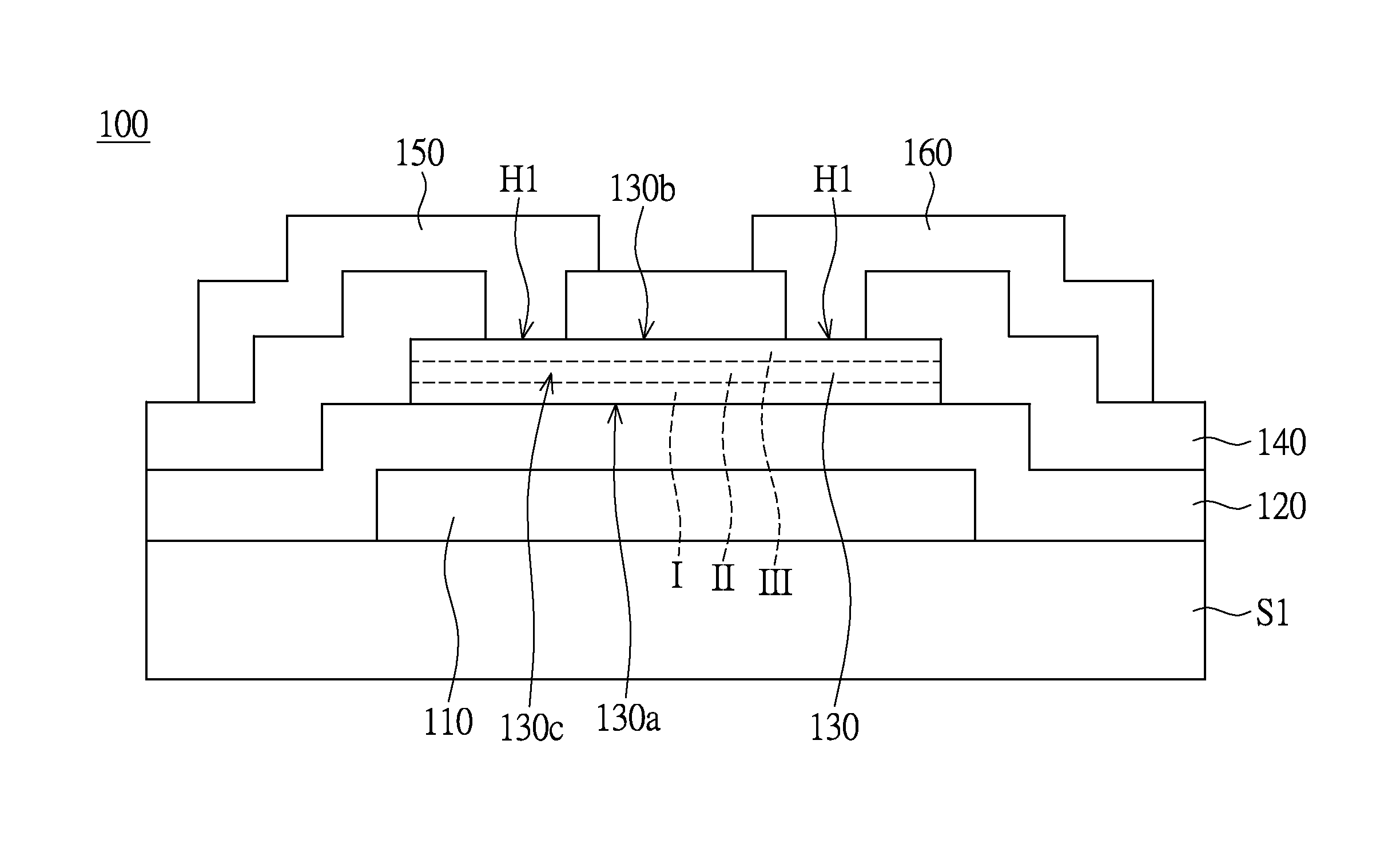
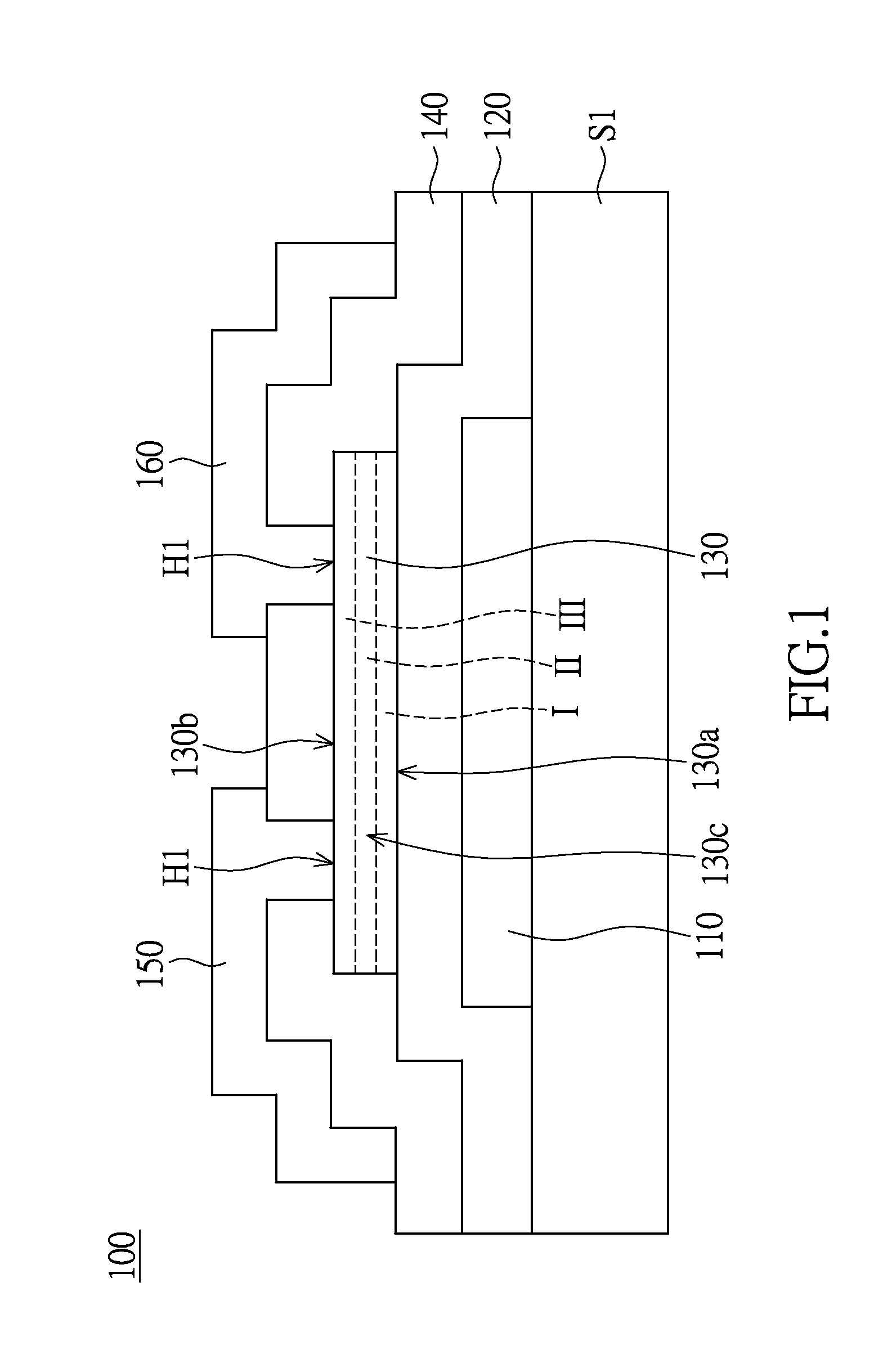
[0023]FIG. 1 illustrates a cross-sectional view of a thin film transistor in accordance with the first embodiment of the present disclosure. Please refer to F...


PUM


Abstract

A thin film transistor includes a gate electrode, a gate insulating layer, a source electrode, a drain electrode, and a channel layer. The gate electrode is disposed on a substrate, and the channel layer is electrically insulated from the gate electrode. The gate insulating layer is disposed between the gate electrode and the channel layer. The source electrode and the drain electrode are electrically connected with the channel layer. The channel layer includes a front channel layer proximate to a side of the gate insulating layer, a back channel layer proximate to a side of the source electrode and an intermediate layer between the front channel layer and the back channel layer. The oxygen vacancy concentration of the front channel layer is greater than the oxygen vacancy concentration of the intermediate layer

Description

BACKGROUND[0001]1. Field of the Invention[0002]The instant disclosure relates to a structure of a thin film transistor, in particular, relates to a thin film transistor compatible with a display panel.[0003]2. Description of Related Art[0004]Most thin film transistor liquid crystal displays include an active element array substrate, a color filter substrate, and a backlight module. The active element array substrate is formed by disposing thin film transistors that control voltage of sub-pixels, so as to adjust the angle of the rotation of liquid crystal. Then, the gray scale (brightness) of sub-pixels can also be adjusted by polarizer films. Through the color filter compatible with the grey scale of sub-pixels, the sub-pixels emitting red, blue and green light can produce imagery.[0005]When voltage is applied to a thin film transistor, if the curve of current change with applied voltages from high to low does not match with that of current change with applied voltages from low to h...

Claims


Application Information

Patent Timeline
Patent Type & Authority Applications(United States)
IPC IPC(8): H01L29/786H01L27/12H01L29/24H01L29/423
CPCH01L29/7869H01L29/24H01L29/78696H01L29/42384H01L27/1225H01L29/42356H01L29/78606
Inventor LEE, KUAN-FENGCHIANG, KUO-CHANGYAN, TZU-MIN
Owner INNOLUX CORP
Why Eureka
Try Eureka