

Thin film transistor substrate and display device using the same
a technology of thin film transistors and substrates, applied in the direction of transistors, semiconductor devices, electrical equipment, etc., can solve the problems of power consumption limit, and achieve the effect of reducing the number of mask processes and efficient manufacturing processes
- Summary
- Abstract
- Description
- Claims
- Application Information
AI Technical Summary
Benefits of technology
Problems solved by technology
Method used
Image

Examples
first example embodiment
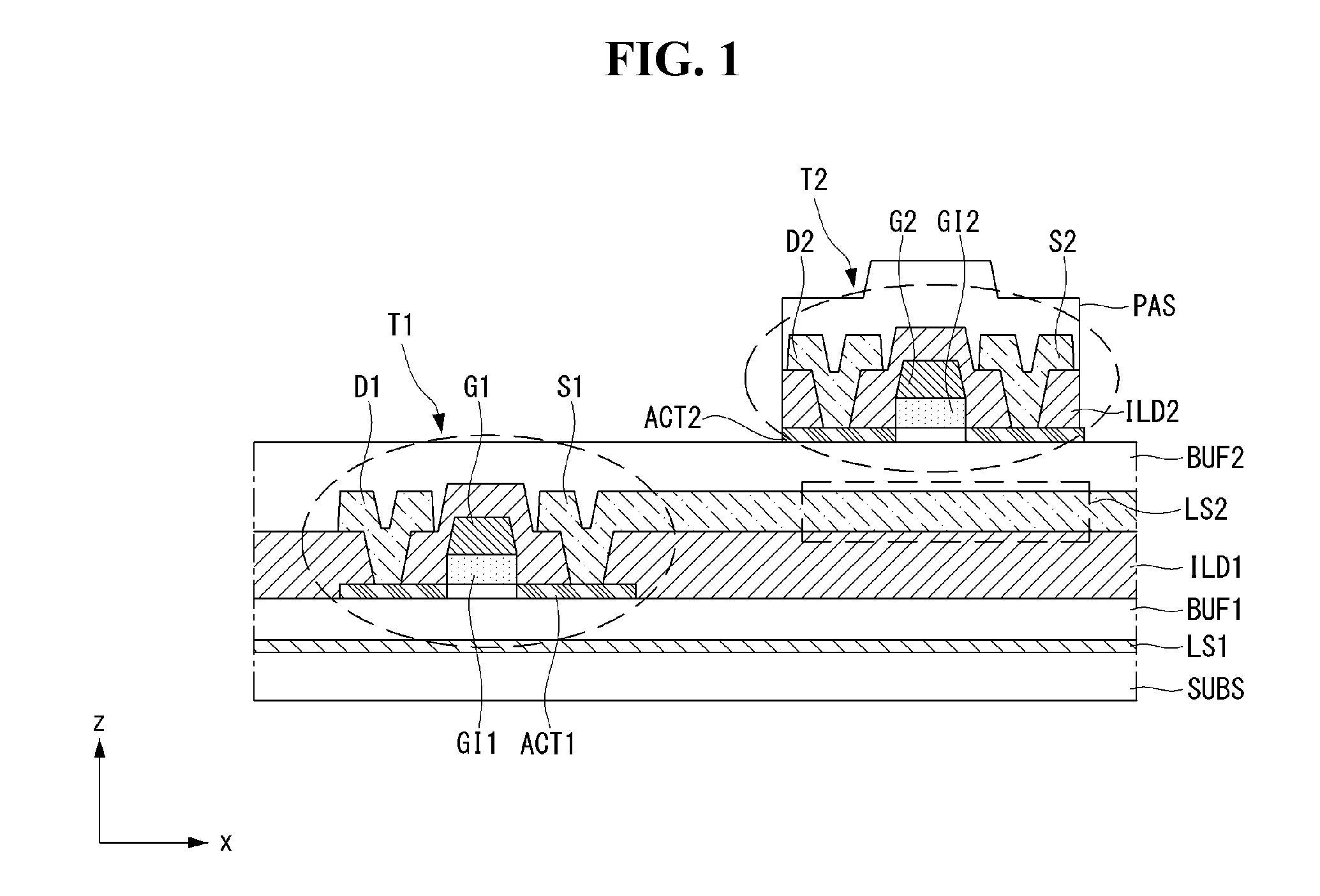
[0036]With reference to FIG. 1, a first example embodiment of the present invention will be explained. FIG. 1 is a cross-sectional view illustrating a thin film transistor (TFT) substrate for a flat panel display according to the first example embodiment of the present invention. Here, the cross sectional views, rather than plane views, are provided to show the main features more clearly.
[0037]As shown in FIG. 1, a thin film transistor (TFT) for a flat panel display according to the first example embodiment of the present disclosure may include a first TFT T1 and a second TFT T2 disposed on a base substrate SUBS (hereinafter referred to as a “substrate”). The first and second TFTs T1 and T2 may have a coplanar structure as illustrated in FIG. 1, but the present disclosure is not limited thereto. For example, the first and second TFTs T1 and T2 may be manufactured with a structure in which bottom-gate and top-gate structures are vertically combined.
[0038]A first semiconductor pattern...
second example embodiment
[0062]FIG. 3 is a cross-sectional view illustrating a thin film transistor (TFT) substrate for a flat panel display according to a second example embodiment of the present invention.
[0063]With reference to FIG. 3, the thin film transistor (TFT) substrate for a flat panel display according to the second embodiment includes a first TFT T1 disposed on a substrate SUBS and a second TFT T2 disposed on the first TFT T1. At least a portion of the second TFT T2 overlaps the first TFT T1 in a thickness direction or in a vertical direction (z).
[0064]A first semiconductor pattern ACT1 of the first TFT T1 includes a polycrystalline semiconductor material, such as LTPS. A first buffer layer BUF1 may be formed on the substrate SUBS and the first semiconductor pattern ACT1 may be formed on the first buffer layer BUF1. A light shield layer may be formed between the substrate SUBS and the first buffer layer BUF1. The first TFT T1 includes a first gate G1 disposed on the first semiconductor pattern A...
third example embodiment
[0072]FIG. 4 is a cross-sectional view illustrating a thin film transistor (TFT) substrate for a flat panel display according to a third example embodiment of the present invention.
[0073]With reference to FIG. 4, the TFT substrate for a flat panel display according to the third embodiment of the present disclosure includes a first TFT T1 disposed on a substrate SUBS and a second TFT T2 disposed on the first TFT T1. At least a portion of the second TFT T2 overlaps the first TFT T1 in a thickness direction or in a vertical direction (z).
[0074]A first semiconductor pattern ACT1 of the first TFT T1 includes a polycrystalline semiconductor material, such as LTPS. A first buffer layer BUF1 may be formed on the substrate SUBS, and the first semiconductor pattern ACT1 may be formed on the first buffer layer BUF1. A light shield layer may be formed between the substrate SUBS and the first buffer layer BUF1. The first TFT T1 includes a first gate G1 disposed on the first semiconductor pattern...
PUM
 Abstract
Description
Claims
Application Information