Image signal processing circuit, image signal processing method, and display unit

a signal processing circuit and image signal technology, applied in the field of image signal processing circuits and image signal processing methods, can solve the problems of increasing the number of man-hours for adjustment, the difficulty of accurately detecting the light emission start voltage shift, and the inability to accurately detect the luminance change greatly affecting image quality degradation on the low-luminance side. , to achieve the effect of accurate correction of the predicted degradation value, and the improvement of the correction accuracy of luminance degradation with time of the display panel

Active Publication Date: 2016-03-24
JOLED INC
View PDF2 Cites 34 Cited by
  • Summary
  • Abstract
  • Description
  • Claims
  • Application Information

AI Technical Summary

Benefits of technology

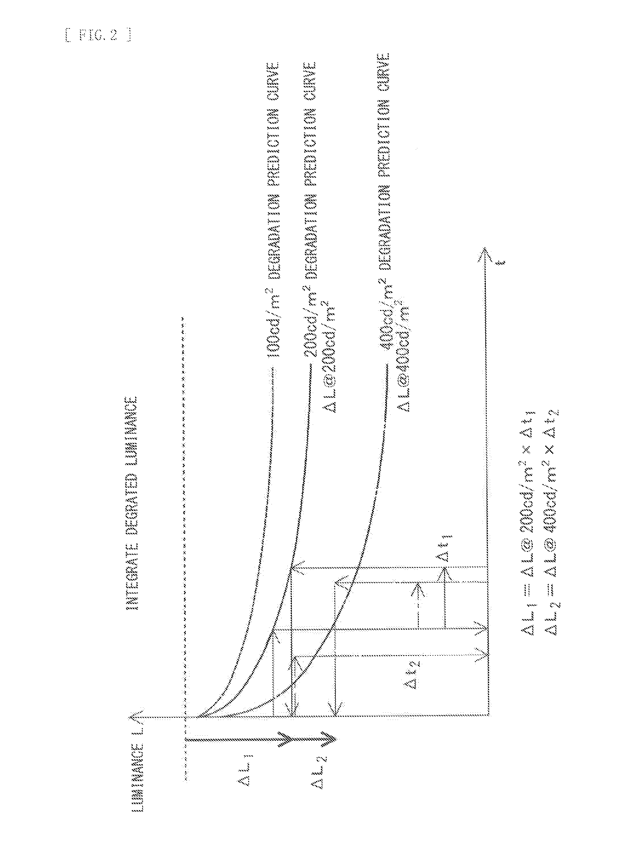
[0023]According to the disclosure, even if an expensive luminance sensor or the like is not used, it is possible to accurately correct variation in the predicted degradation value (estimated value) of the light emission start voltage shift greatly influencing image quality degradation on the low-luminance side; therefore, correction accuracy for the luminance degradation with time of the display panel is allowed to be improved.
[0024]It is to be noted that the effects described in this description are merely examples; therefore, effects are not limited thereto, and may also include additional effect.

Problems solved by technology

However, as with the above-described related art, in measurement of the actual degradation state by the luminance sensor, it is difficult to accurately detect a change in luminance greatly influencing image quality degradation on a low-luminance side, i.e., a voltage shift at light emission state point (a light emission start voltage shift / offset).
Nevertheless, it is not impossible to accurately detect the light emission start voltage shift (gray-scale degradation) with use of the luminance sensor.
However, since, in addition to the necessity of using a large-area luminance sensor with high light reception sensitivity, a luminance sensor having performance substantially equal to that of an expensive measuring instrument is necessary because of the necessity of long-time measurement and the like; therefore, cost and the number of man-hours for adjustment are increased, and an influence of restrictions or the like on convenience in use by a user is increased.

Method used


Image

  • Image signal processing circuit, image signal processing method, and display unit
  • Image signal processing circuit, image signal processing method, and display unit
  • Image signal processing circuit, image signal processing method, and display unit

Examples


modification examples

3. Modification Examples

[0042](General Description of Image Signal Processing Circuit, Image Signal Processing Method, and Display Unit of Disclosure)

[0043]An image signal processing circuit or an image signal processing method of the disclosure is suitably used in a display unit in which a light emission section of an effective pixel contributing to image display is configured of a current-driven light-emitting device of which light emission is controlled according to intensity (magnitude) of a current. As the current-driven light-emitting device, for example, an organic electroluminescence device (hereinafter referred to as “organic EL device”) using a phenomenon in which light is emitted in response to application of an electric field to an organic thin film may be used. Examples of the current-driven light-emitting device may include not only the organic EL device but also an inorganic EL device, an LED device, and a laser diode device.

[0044]The organic EL display unit using the...


PUM


Abstract

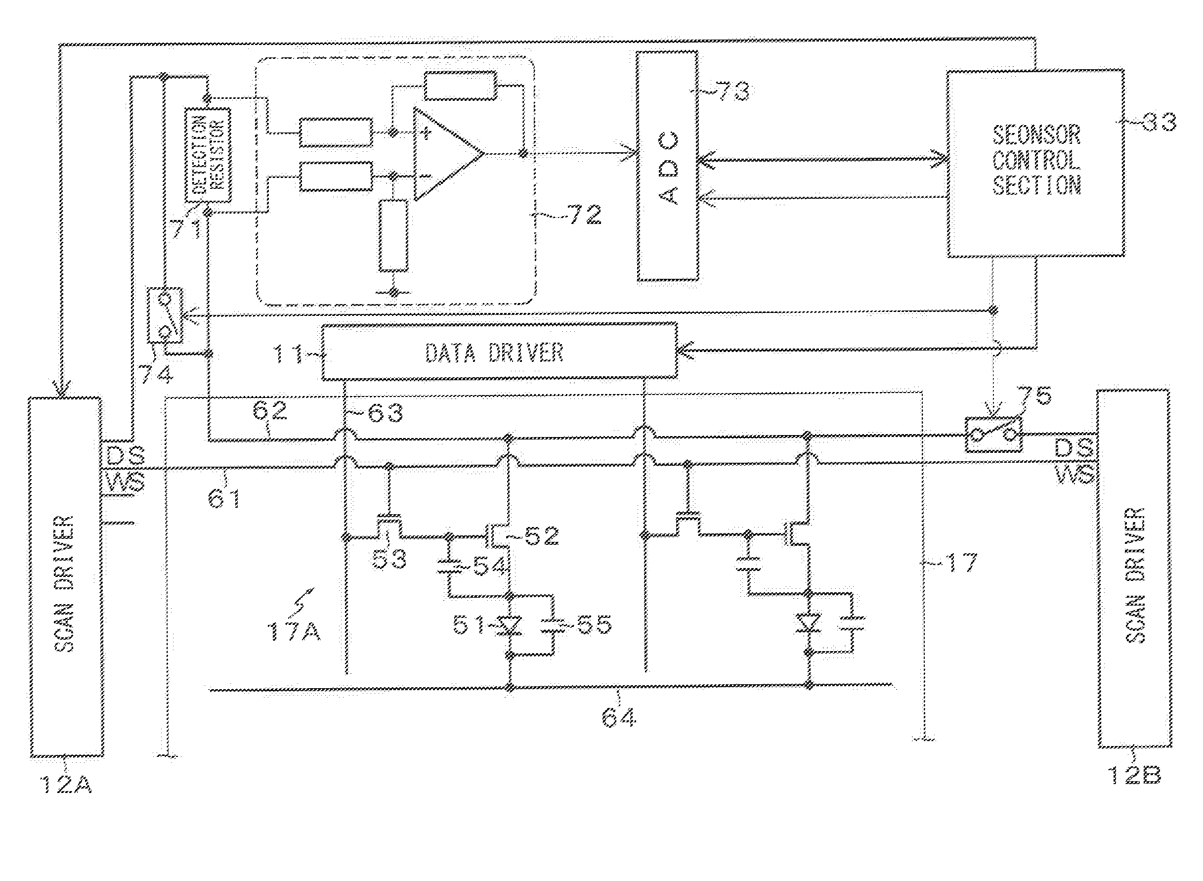
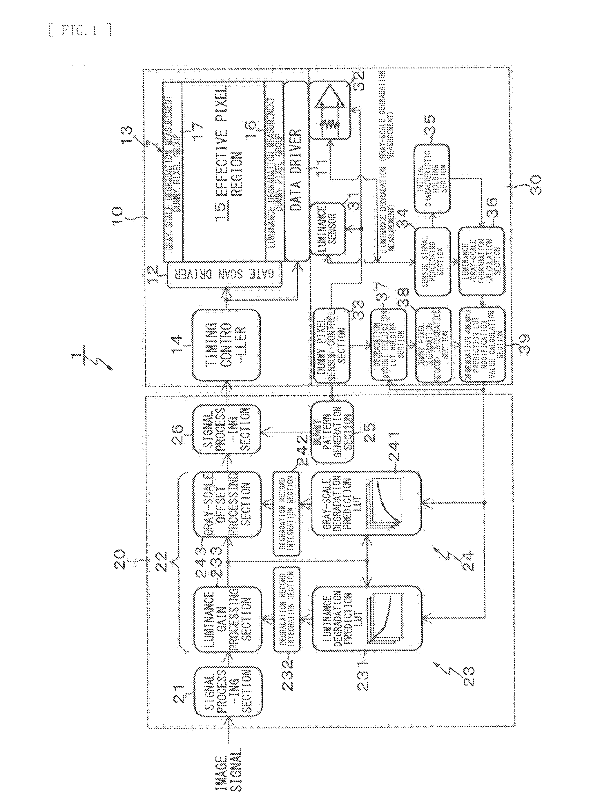
An image signal processing circuit includes: a display panel including a first dummy pixel provided outside an effective pixel region; a current detection section configured to detect a change in a current in the first dummy pixel; a modification processing section configured to modify a predetermined predicted degradation value, based on an actual degradation amount of the current detected by the current detection section; and a correction processing section configured to correct an image signal, based on the predicted degradation value modified by the modification processing section, the image signal being adapted to drive an effective pixel.

Description

TECHNICAL FIELD[0001]The disclosure relates to an image signal processing circuit, an image signal processing method, and a display unit.BACKGROUND ART[0002]In a display unit, more specifically, a flat panel (planar) display unit, luminance degradation with time of a display panel is corrected, based on a degradation value (a predicted degradation value) predicted from information of a pixel signal and typical degradation characteristics of the display panel. However, since the degradation characteristics vary for each display panel, it is not possible to sufficiently correct the degradation, based on a typical predicted degradation value (an estimated value) only.[0003]As a countermeasure, there has been proposed technology in which an actual luminance degradation state of each display panel is measured with use of a dummy pixel by a luminance sensor, and a predicted degradation value (an estimated value) is adjusted at regular intervals, based on a thus-obtained measurement result...

Claims


Application Information

Patent Timeline
Patent Type & Authority Applications(United States)
IPC IPC(8): G09G3/32
CPCG09G3/3258G09G2300/0413G09G2330/12G09G2320/043G09G2320/0233G09G2330/026G09G3/3233G09G2320/029
Inventor MAEYAMA, KOICHI
Owner JOLED INC
Why Eureka
Try Eureka