Semiconductor light-emitting device, method for producing same, and display device

a technology of semiconductor light-emitting devices and display devices, which is applied in the direction of semiconductor devices, basic electric elements, electrical appliances, etc., can solve the problems of difficult to reduce the size of the display device, process that requires considerable time and labor, and impede the reduction in the size of the semiconductor light-emitting device, etc., to achieve the effect of small size, reduced cost and manufactured in a smaller siz

Active Publication Date: 2016-03-24
ROHM CO LTD
View PDF6 Cites 3 Cited by
  • Summary
  • Abstract
  • Description
  • Claims
  • Application Information

AI Technical Summary

Benefits of technology

The present invention provides a semiconductor light-emitting device that can be made smaller in size, and a method of manufacturing the device. Additionally, the invention provides a display device that can be made smaller in size and at a lower cost. The surface roughness of the device helps to improve bonding strength, preventing separation between the device and the resin package, which allows for a smaller size. The invention also simplifies the manufacturing process by eliminating the need for a light-transmissive resin filling the space between reflecting surfaces, reducing manufacturing costs and making the display device smaller in size.

Problems solved by technology

This is another obstacle that impedes the reduction in size of the semiconductor light-emitting device 901.
However, this process requires considerable time and labor, and hence constitutes a bottleneck from the viewpoint of production efficiency of the display device 902.
Therefore, it has been difficult to reduce the size of the display device 902, and to improve the definition thereof.

Method used


Image

  • Semiconductor light-emitting device, method for producing same, and display device
  • Semiconductor light-emitting device, method for producing same, and display device
  • Semiconductor light-emitting device, method for producing same, and display device

Examples


Embodiment Construction

[0058]Preferred embodiments of the present invention will be described below with reference to the accompanying drawings.

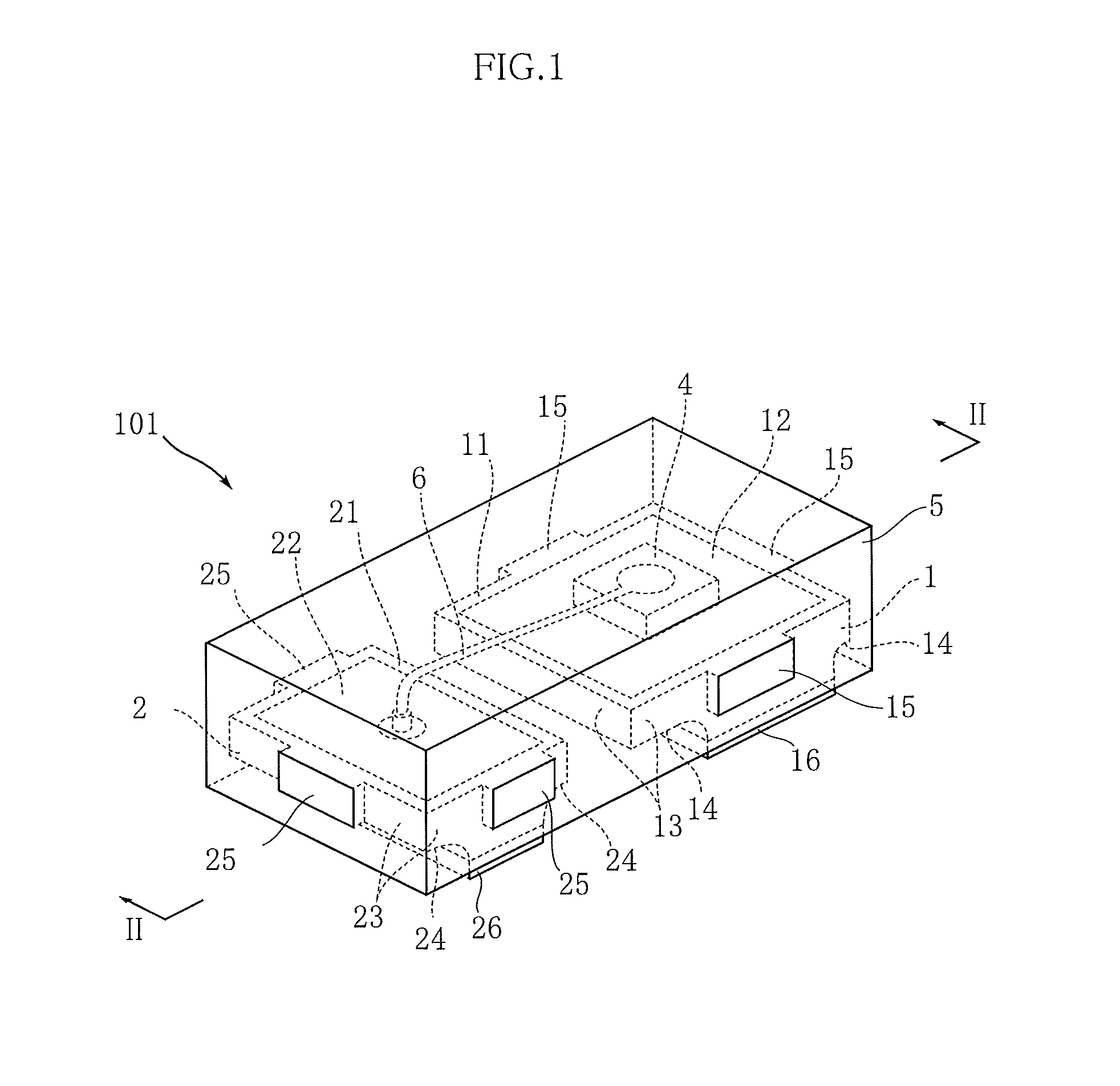
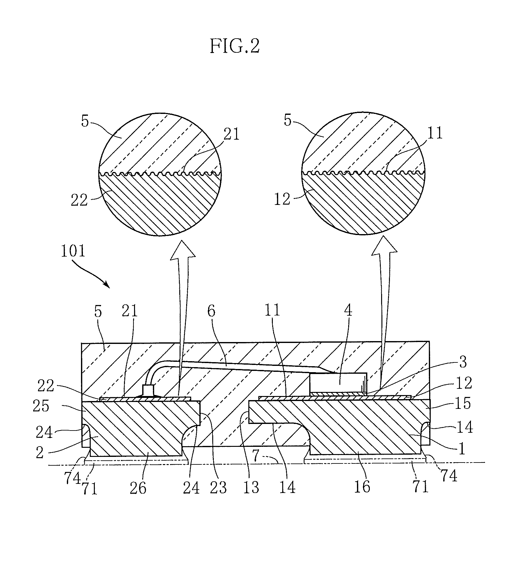
[0059]FIGS. 1 to 3 depict an example of a semiconductor light-emitting device according to an embodiment of the present invention. The semiconductor light-emitting device 101 according to this embodiment includes a pair of leads 1, 2, a metal joint layer 3, an LED chip 4, and a resin package 5. In FIG. 1, the metal joint layer 3 is not shown for the sake of convenience. The semiconductor light-emitting device 101 is configured as a small and thin device, having dimensions of approximately 0.6 mm in length, 0.3 mm in width, and 0.2 mm in thickness.

[0060]The pair of leads 1, 2 serve to support the LED chip 4 and supply power thereto. The leads 1, 2 are formed of Cu or an alloy thereof, in a thickness of slightly less than 0.1 mm. The lead 1 includes a main surface 11, four side faces 13, two buried surfaces 14, three drawn-out portions 15, and a mounting terminal 16...


PUM


Abstract

A semiconductor light-emitting device (101) includes an LED chip (4), a lead (1) having a main surface (11) on which the LED chip (4) is mounted, and a resin package (5) covering the LED chip (4). The main surface (11) is roughened, and the main surface (11) is held in contact with the resin package (5). These configurations contribute to the downsizing of the semiconductor light-emitting device (101).

Description

[0001]This application is a Continuation of U.S. Ser. No. 13 / 819,830, filed Feb. 28, 2013, which is a National Stage Application of PCT / JP2011 / 071248, filed Sep. 16, 2011, which applications are incorporated herein by reference.TECHNICAL FIELD[0002]The present invention relates to a semiconductor light-emitting device including semiconductor light-emitting elements, while also relating to a manufacturing method thereof and a display device such as a 7-segment display and a dot matrix display.BACKGROUND ART[0003]FIG. 17 depicts a conventional semiconductor light-emitting device (see e.g. Patent document 1). The semiconductor light-emitting device 901 shown in FIG. 17 includes an LED chip 912 bonded on a substrate 910. The LED chip 912 and a wire 913 are encapsulated in a resin package 914.[0004]In recent years, there has been a growing demand for reduction in size, for example with respect to mobile phones. Accordingly, the semiconductor light-emitting device 901 is required to be ma...

Claims


Application Information

Patent Timeline
Patent Type & Authority Applications(United States)
IPC IPC(8): H01L33/62H01L33/22H01L33/54
CPCH01L33/62H01L33/22H01L33/54H01L24/48H01L24/73H01L24/97H01L33/486H01L33/60H01L2224/32245H01L2224/48091H01L2224/48247H01L2224/48471H01L2224/73265H01L2224/97H01L2924/00014H01L2924/01004H01L2924/01029H01L2924/01032H01L2924/01033H01L2924/01047H01L2924/0105H01L2924/01079H01L2924/01082H01L2924/01088H01L2924/01322H01L2924/014H01L2924/181H01L2924/00012H01L2924/00H01L2224/45099H01L2224/05599H01L25/0753H01L33/08H01L33/50H01L33/507H01L33/52H01L33/56H01L2933/005H01L2933/0066
Inventor MINESHITA, KENTARO
Owner ROHM CO LTD
Why Eureka
Try Eureka