Method for performing activation of dopants in a gan-base semiconductor layer

Active Publication Date: 2016-03-31
COMMISSARIAT A LENERGIE ATOMIQUE ET AUX ENERGIES ALTERNATIVES
View PDF4 Cites 4 Cited by
  • Summary
  • Abstract
  • Description
  • Claims
  • Application Information

AI Technical Summary

Benefits of technology

[0012]It is observed that a requirement exists to provide a method for performing activation of p-type dopants in a GaN-base semiconductor

Problems solved by technology

However performing annealing at such a high pressure is only possible if a suitable device is available which limits the advantages of such a method.
If the heat treatment is not performed at high pressure, the surface of th

Method used


Image

  • Method for performing activation of dopants in a gan-base semiconductor layer
  • Method for performing activation of dopants in a gan-base semiconductor layer
  • Method for performing activation of dopants in a gan-base semiconductor layer

Examples


first embodiment

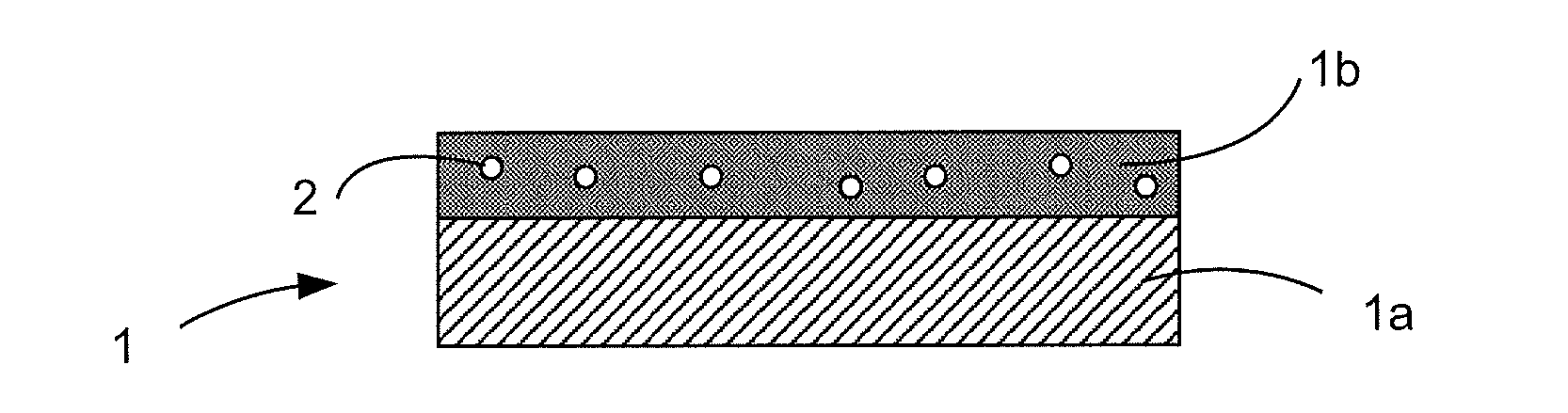
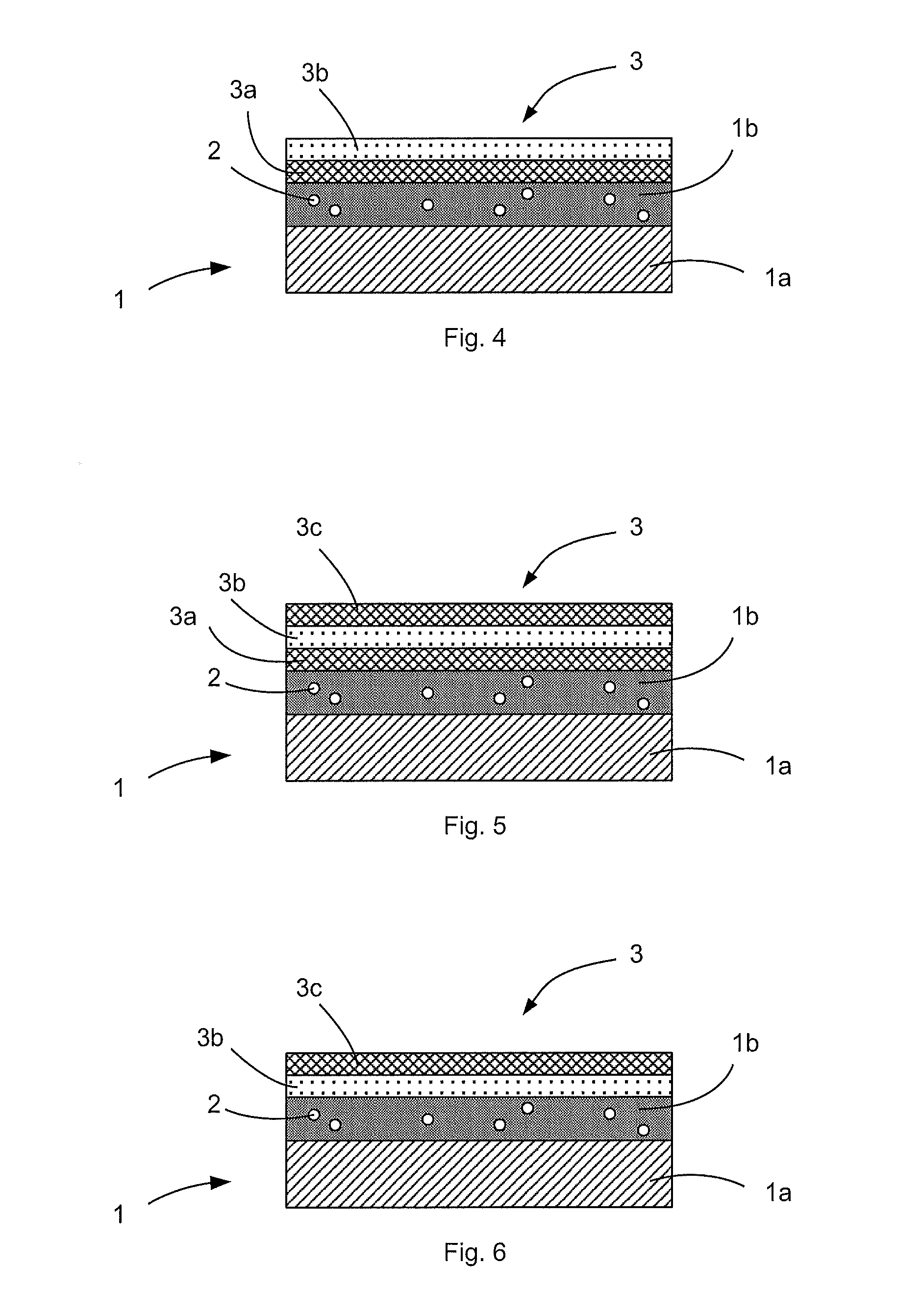
[0054] illustrated in FIG. 4, cap block 3 comprises an AlGaN or AlN layer 3a in contact with semiconductor material layer 1b, and a Mg or MgO layer 3b in contact with layer 3a.

[0055]The Mg or MgO layer acts as a reservoir of Mg atoms which constitute p-type dopant impurities able to diffuse through AlGaN layer 3a to semiconductor material layer 1b. The AlGaN layer also prevents diffusion to semiconductor material layer 1b of species belonging to other layers able to be deposited above layer 3b.

[0056]Deposition of AlGaN layer 3a is advantageously performed by means of a similar method to the one that has just been described in relation with n-type doping. The thickness of AlGaN layer 3a is comprised between 1 and 40 nm, preferentially between 5 and 20 nm and ideally equal to 10 nm. This thickness range enables a sufficiently weak layer 3a to be had to allow diffusion of the Mg atoms in the direction of layer 1b and ensures a sufficient thickness to perform the barrier function for ...

fourth embodiment

[0069]According to cap block 3 used for p-doping of semiconductor material layer 1b, the cap block can contain a single Mg or MgO layer 3b (cf. FIG. 7). In this case, it can be advantageous to deposit a layer 3b having a thickness of more than 10 nm for cap block 3 to be able to play its role of protection barrier correctly when the heat treatment is performed.

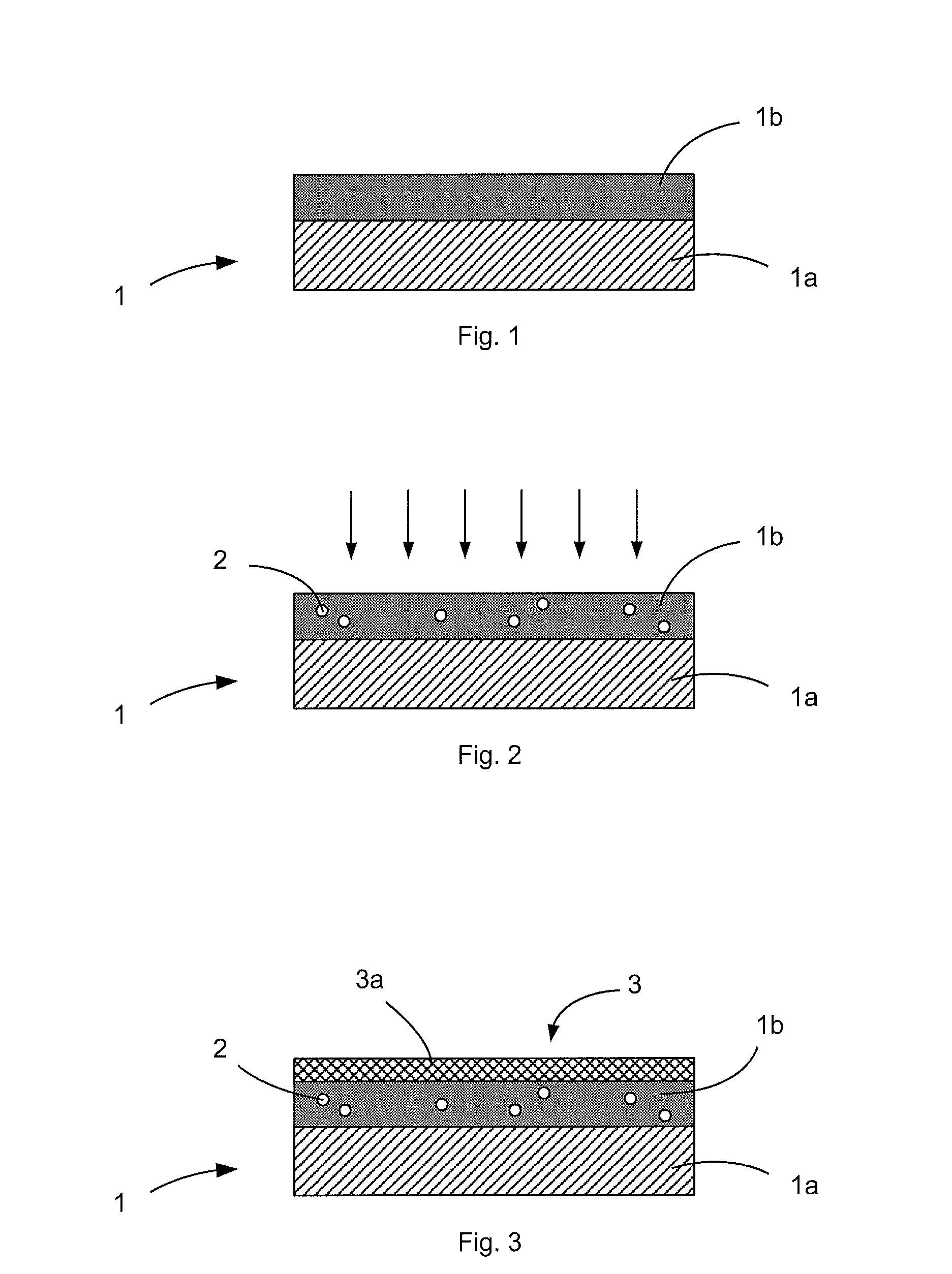
[0070]Whether the doping performed is n-type or p-type, a silicon-base covering layer 4 is deposited on top of cap block 3. This step is illustrated in FIG. 8.

[0071]Covering layer 4 can be made from amorphous silicon, silicon oxide, or silicon nitride which may be stoichiometric or not and noted SixNy. Layer 4 can advantageously be made from SiO2, as this material is very resistant when temperature changes take place.

[0072]When the method is used to activate n-type dopants, it is not necessary for cap block 3 to be provided with a Mg or MgO layer. In this case, Si atoms can diffuse through cap block 3 in the direction of semic...


PUM


Abstract

The method for performing activation of p-type dopants in a GaN-base semiconductor comprises a first step consisting in providing a substrate comprising (i) a GaN-base semiconductor material layer comprising p-type electric dopant impurities, (ii) a cap block devoid of any silicon-base compound, in contact with the semiconductor material layer, and (iii) a silicon-base covering layer covering the cap block. The method comprises a second heat treatment step at a temperature of more than 900° C. so as to activate the p-type electric dopant impurities in the semiconductor material layer.

Description

BACKGROUND OF THE INVENTION[0001]The invention relates to a method for performing activation of dopants in a semiconductor layer.STATE OF THE ART[0002]Ion implantation is commonly used to dope semiconductors. The ions used for doping are generally produced from a gaseous or solid source and impact the semiconductor after they have been accelerated, for example, with an energy comprised between 10 and 500 keV.[0003]Once implantation has been terminated, the doped semiconductor undergoes heat treatment designed to both restore the crystal quality of the semiconductor and to activate the dopants, i.e. to enable them to take the place of certain atoms of the crystal lattice of the semiconductor. The thermal budget applied also results in diffusion of the latter into the semiconductor.[0004]For example, to obtain a high Si+ ion (n-doping) or Mg+ ion (p-doping) activation ratio in a GaN semiconductor layer, one solution can be to perform heat treatment of the material without covering it ...

Claims


Application Information

Patent Timeline
IPC IPC(8): H01L21/324H01L21/225H01L29/20
CPCH01L21/3245H01L29/2003H01L21/2258H01L21/26553
Inventor AGRAFFEIL, CLAIRE
Owner COMMISSARIAT A LENERGIE ATOMIQUE ET AUX ENERGIES ALTERNATIVES
Why Eureka
Try Eureka