Silicon carbide semiconductor device and process for producing the same

Inactive Publication Date: 2006-10-05
PANASONIC CORP
View PDF20 Cites 63 Cited by
  • Summary
  • Abstract
  • Description
  • Claims
  • Application Information

AI Technical Summary

Benefits of technology

[0042] Thus, the method for fabricating the semiconductor device according to the present invention allows a silicon carbide semiconductor

Problems solved by technology

However, since the silicon carbide substrate is processed at a high temperature in the step shown in FIG. 9(d), macro-steps 145 are formed disadvantageously in the upper surface of the region into which the ions have been implanted.
In a prior art technology as shown in FIGS. 9, projections and depressions formed due to the macro-steps in the upper surface of the silicon carbide thin film after the activation annealing have presented a great obstacle to an improvement in the performance of the semiconductor device.
The formation of the macro-steps has caused performance degradation in numerous semiconductor devices including a MOSFET.
In the case with, e.g., a Schottky diode, the problem is encountered that the localization of an electric field to the tip portions of macro-steps occurs in a Schottky electrode formed on the upper surface of a silicon carbide thin film and the breakdown voltage t

Method used


Image

  • Silicon carbide semiconductor device and process for producing the same
  • Silicon carbide semiconductor device and process for producing the same
  • Silicon carbide semiconductor device and process for producing the same

Examples


Example

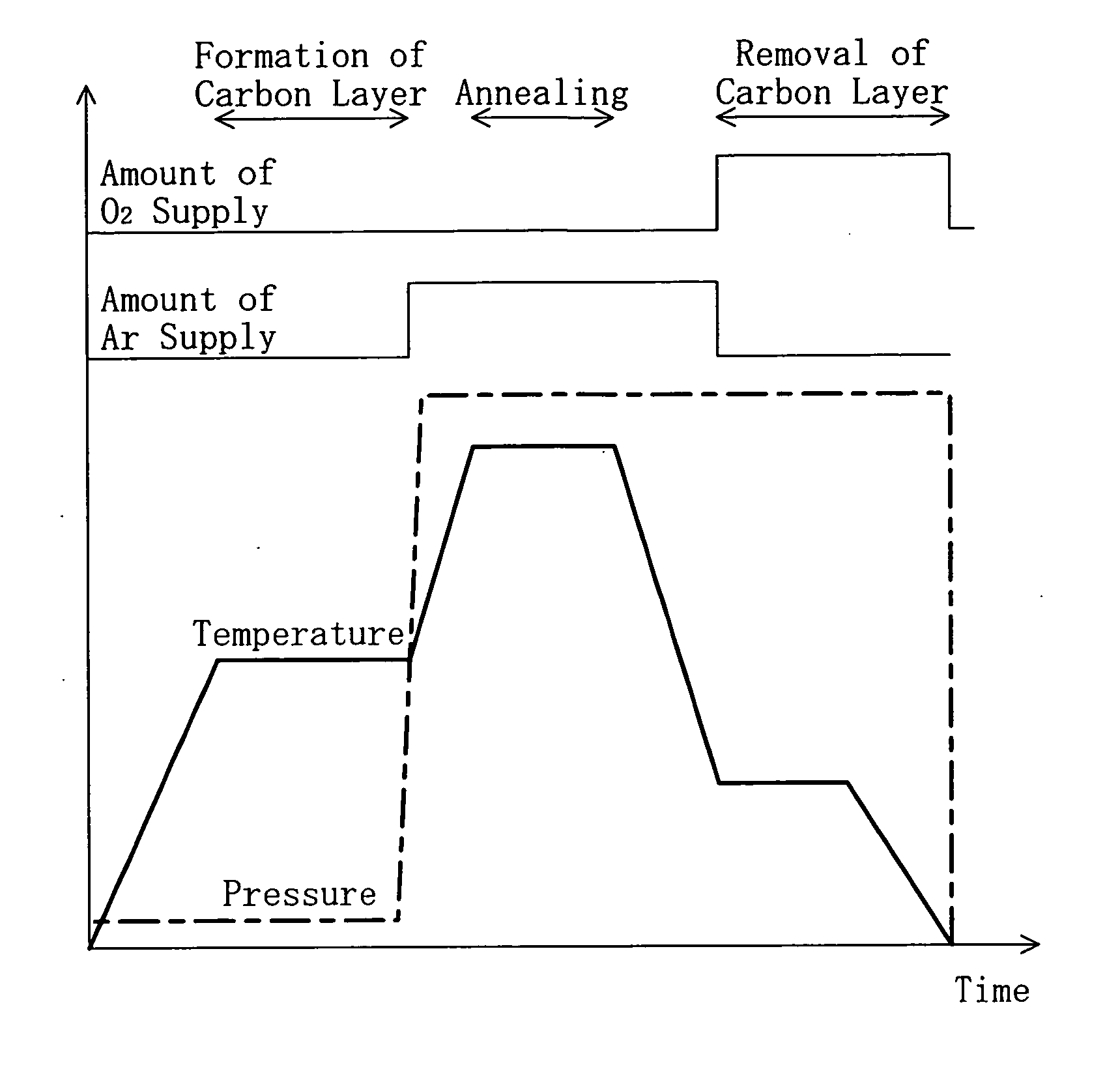
[0082] A method for fabricating a semiconductor device according to a first embodiment of the present invention is characterized in that a carbon layer is formed on a substrate surface by performing annealing in a reduced pressure atmosphere before an activation annealing process after ion implantation and then the activation annealing is performed continuously by raising a pressure and a temperature. Referring to the drawings, the semiconductor device and the method for fabricating the same according to the first embodiment will be described herein below.

[0083]FIG. 10 is a cross-sectional view showing the structure of an annealing furnace used in the method for fabricating the semiconductor device according to the present invention. As shown in the drawing, the annealing furnace comprises: a reaction furnace 150; a susceptor 152 made of carbon which is for fixing a substrate 151; a support shaft 153; a coil 154 for heating a sample; a gas supply system 158 for supplying an argon g...

Example

[0108] As a second embodiment of the present invention, a silicon carbide MOSFET having a step height of 1 nm or less at the upper surface of the layer into which an impurity has been introduced, which is an example of the silicon carbide semiconductor device, and a method for fabricating the same will be described with reference to the drawings.

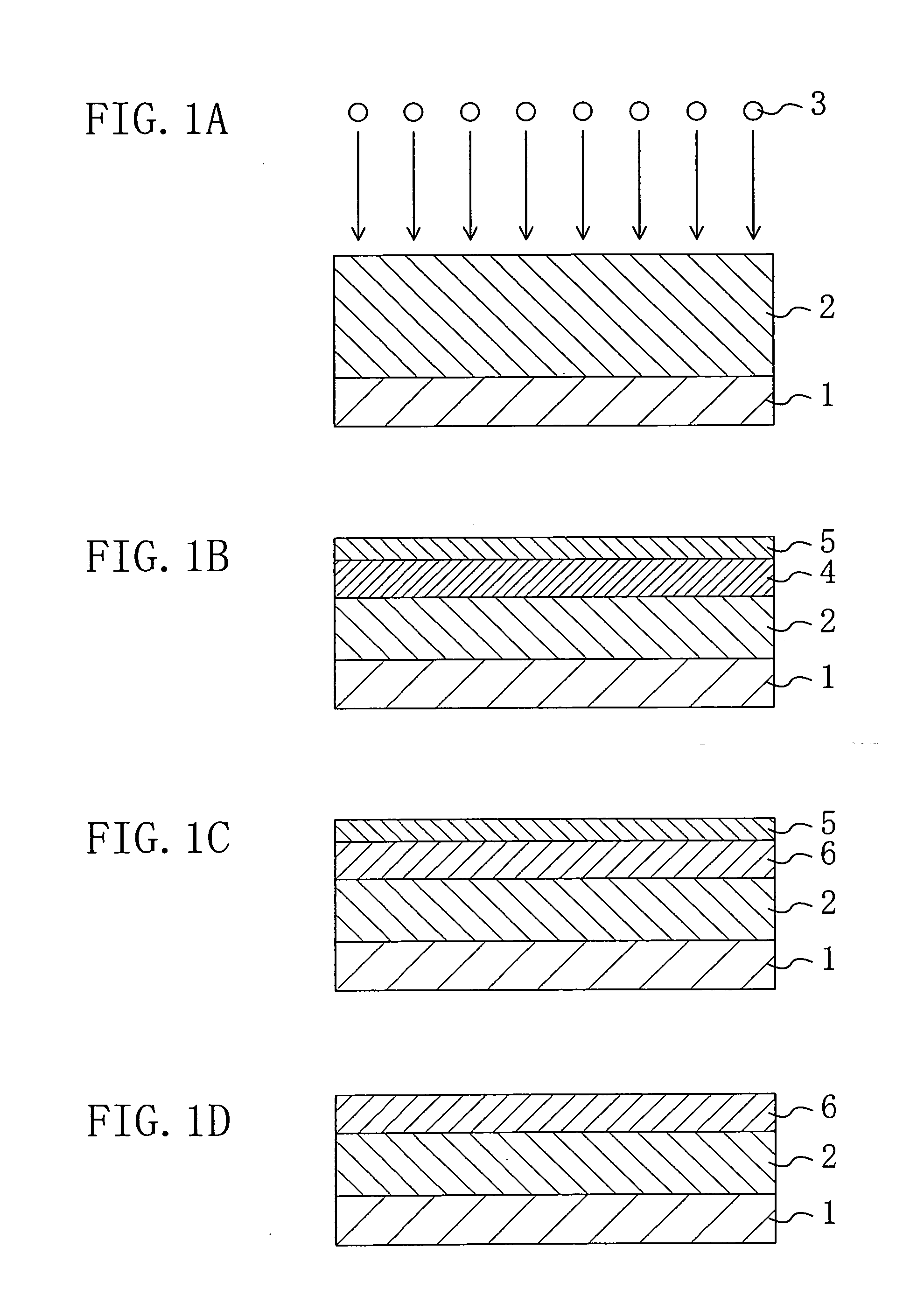
[0109] FIGS. 5(a) to 5(c) and FIGS. 6(a) to 6(c) are cross-sectional views illustrating the method for fabricating the silicon carbide MOSFET according to the present embodiment.

[0110] First, in the step shown in FIG. 5(a), a silicon carbide substrate 21 is prepared. As the silicon carbide substrate 21, there is used, e.g., a 4H—SiC substrate 1 having a principal surface thereof tilted at an off-angle of 8 degrees in the [11-20] (112-bar 0) direction from the (0001) plane and with a diameter of 50 mm. The substrate is of an n-type and the concentration of carriers therein is 1×1018 cm−3.

[0111] Next, an n-type impurity doped layer is grown...


PUM


Abstract

A method for fabricating a semiconductor device includes the steps of implanting ions into a silicon carbide thin film (2) formed on a silicon carbide substrate (1), heating the silicon carbide substrate in a reduced pressure atmosphere to form a carbon layer (5) on the surface of the silicon carbide substrate, and performing activation annealing with respect to the silicon carbide substrate in an atmosphere under a pressure higher than in the step of forming the carbon layer (5) and at a temperature higher than in the step of forming the carbon layer (5).

Description

TECHNICAL FIELD [0001] The present invention relates to a semiconductor device using a silicon carbide substrate and to a method for fabricating the same. BACKGROUND ART [0002] Silicon carbide (SiC) is a semiconductor material the application of which to a next-generation low-loss power device or the like is expected because it features a larger band gap than silicon (Si) and a higher field intensity at which a dielectric breakdown occurs. Silicon carbide has numerous polytypes including cubic-type 3C—SiC and hexagonal-type 6H—SiC and 4H—SiC. Of these polytypes, 6H—SiC and 4H—SiC are used commonly to produce practically usable silicon carbide semiconductor devices. Among them, a silicon carbide substrate (SiC substrate) having a principal surface which is substantially coincident with the (0001) plane perpendicular to the crystal axis of the c-axis is used mostly for a silicon carbide semiconductor device (SiC semiconductor device). [0003] To form a silicon carbide semiconductor dev...

Claims


Application Information

Patent Timeline
IPC IPC(8): H01L31/0312H01L21/265H01L21/04
CPCH01L21/046H01L21/324H01L29/1608H01L29/66068
Inventor TAKAHASHI, KUNIMASAKITABATAKE, MAKOTOYAMASHITA, KENYAUCHIDA, MASAOKUSUMOTO, OSAMUMIYANAGA, RYOKO
Owner PANASONIC CORP
Why Eureka
Try Eureka