Touch panel and touch display apparatus including the same
- Summary
- Abstract
- Description
- Claims
- Application Information
AI Technical Summary
Benefits of technology
Problems solved by technology
Method used
Image


Examples
example 1
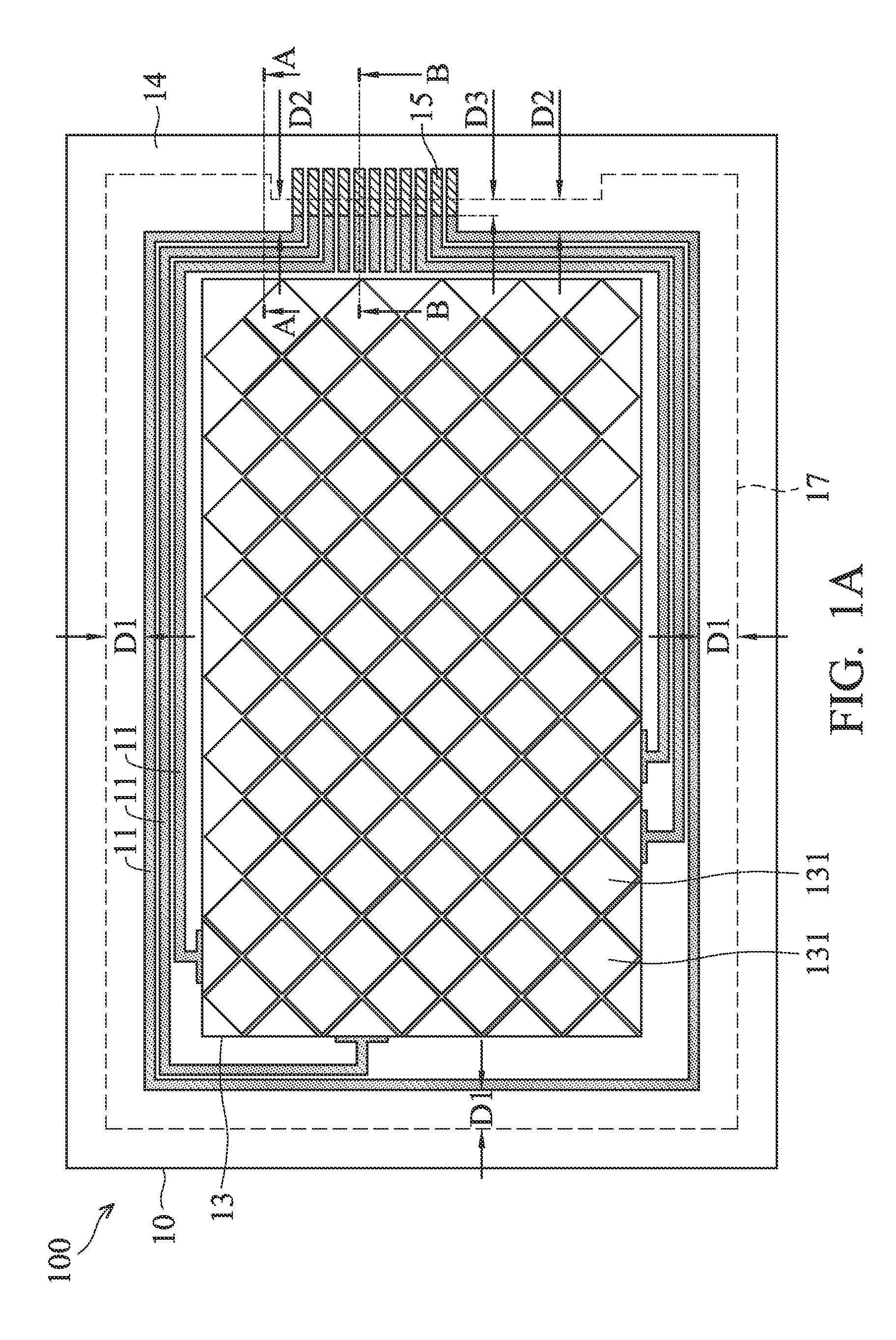
[0039]Bonding pads and metal traces were formed on a substrate corresponding to FIG. 1A, wherein the terminals of the metal traces were located on the bonding pads. In this example, the bonding pads were ITO, metal traces were a bi-layer structure of aluminum / molybdenum, and the substrate was glass. The bonding pads and the metal traces were formed by general processes such as deposition, lithography, etching, and the like.
[0040]A passivation layer was formed to cover the metal traces and the substrate. In this example, the passivation layer was photo curable resin formed by lithography. As shown in FIG. 1A, a distance D3 between the metal traces on the bonding pads and the edge of the passivation layer was 50 micrometers.
[0041]The touch panel was tested under a relative humidity of 85% and a temperature of 85° C. to measure the electrical properties of the metal traces after 144 hours, 288 hours, and 500 hours, respectively. The results are tabulated in Table 1.
example 2
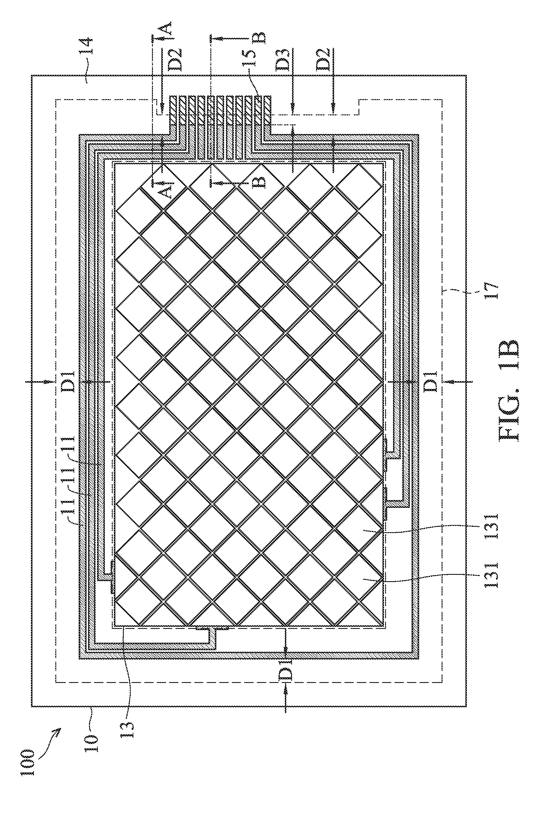
[0042]Example 2 was similar to Example 1. The difference in Example 2 was the distance D3 between the metal traces on the bonding pads and the edge of the passivation layer being 100 micrometers. The other factors such as the materials and formation processes of the substrate, the bonding pads, the metal traces, and the passivation layer were the same as that in Example 1. The touch panel was tested under a relative humidity of 85% and a temperature of 85° C. to measure the electrical property of the metal traces after 144 hours, 288 hours, and 500 hours, respectively. The results are tabulated in Table 1.
example 3
[0043]Example 3 was similar to Example 1. The difference in Example 3 was the distance D3 between the metal traces on the bonding pads and the edge of the passivation layer being 131 micrometers. The other factors such as the materials and formation processes of the substrate, the bonding pads, the metal traces, and the passivation layer were the same as that in Example 1. The touch panel was tested under a relative humidity of 85% and a temperature of 85° C. to measure the electrical property of the metal traces after 144 hours, 288 hours, and 500 hours, respectively. The results are tabulated in Table 1.
PUM
 Abstract
Description
Claims
Application Information
PatSnap Eureka turns technology decisions into work you can execute. Powered by our Innovation Knowledge Graph, it runs expert workflows across engineering, life sciences, materials and intellectual property. Get your review-ready output in minutes.


