Multilayer ceramic electronic component

a technology of electronic components and ceramics, applied in the direction of fixed capacitor details, stacked capacitors, fixed capacitors, etc., can solve problems such as separation problems

Active Publication Date: 2016-05-19
MURATA MFG CO LTD
View PDF1 Cites 33 Cited by
  • Summary
  • Abstract
  • Description
  • Claims
  • Application Information

AI Technical Summary

Benefits of technology

[0022]According to various preferred embodiments of the present invention, multilayer ceramic electronic components having good adhesive force between a conductive resin layer and a sintered metal layer are provided.

Problems solved by technology

In the multilayer ceramic electronic component, the conductive resin electrode layer is formed between the sintered electrode layer and the plating layer, thereby resolving to some extent the problem of cracks being caused in the ceramic element body due to a temperature cycle during use and the problem of weakening resistance to deflection of a substrate when the multilayer ceramic electric component is mounted on the substrate.
Therefore, deflection of a substrate on which the multilayer ceramic electronic component is mounted is absorbed by the conductive resin electrode layer, but the low adhesive force between the conductive resin electrode layer and the sintered electrode layer causes the problem of separation between the conductive resin electrode layer and the sintered electrode layer.

Method used


Image

  • Multilayer ceramic electronic component
  • Multilayer ceramic electronic component
  • Multilayer ceramic electronic component

Examples


experimental examples

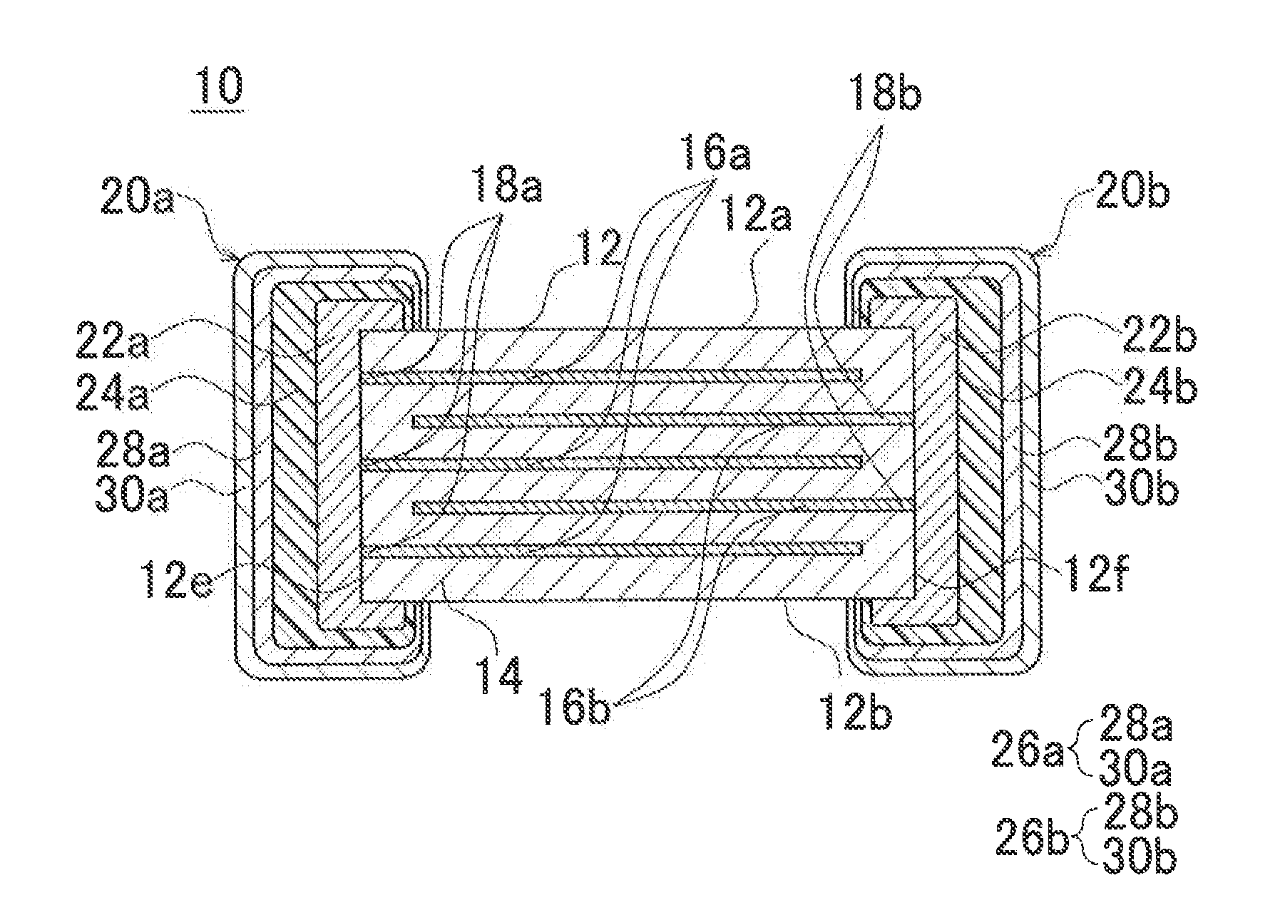
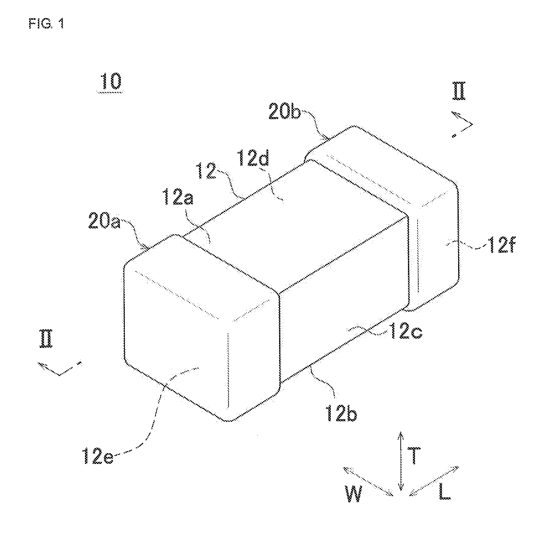
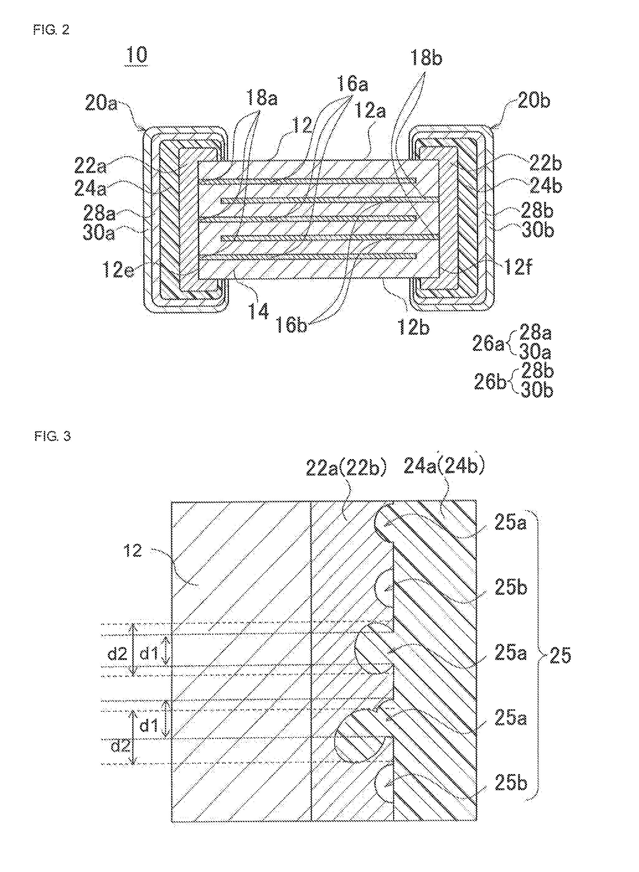
[0102]As an example, 20 multilayer ceramic capacitors 10 according to a preferred embodiment of the present invention described above were formed.

[0103]As a comparative example, 20 multilayer ceramic capacitors each having 2 or more recesses within a length of 70 μm at an interface (first interface) between a sintered metal layer and a conductive resin layer were formed. The multilayer ceramic capacitors had the same design structure except the number of recesses.

[0104]Each of the multilayer ceramic capacitors was mounted on a substrate, and the substrate was deflected. In this case, separation occurred between the sintered metal layer and the conductive resin layer of each of 5 multilayer ceramic capacitors among the 20 multilayer ceramic capacitors of the comparative example. On the other hand, in each of the multilayer ceramic capacitors of the example, deflection occurred at the interface (first interface) between the sintered metal layer and the conductive resin layer.

[0105]Alt...


PUM

PropertyMeasurementUnit
lengthaaaaaaaaaa
thicknessaaaaaaaaaa
thicknessaaaaaaaaaa

Abstract

A multilayer ceramic capacitor includes a ceramic element body including internal electrodes therein. External electrodes are provided on end surfaces of the ceramic element body and electrically connected to exposed portions of respective ones of the internal electrodes. Each of the external electrodes includes a sintered metal layer, a conductive resin layer, and a plating layer. In a cross section including a first interface between the sintered metal layer and the conductive resin layer, the sintered metal layer includes a plurality of recesses each including an inlet extending along the first interface and an inner portion extending from the first interface into the sintered metal layer, each of the recesses having a shape in which a dimension of the inner portion is larger than a dimension of the inlet measured along the first interface, and in a cross section including a second interface between the conductive resin layer and the plating layer, a number of the metal particles exposed from the conductive resin layer in a portion of the second interface with a length of about 1 mm is 50 to 250.

Description

BACKGROUND OF THE INVENTION[0001]1. Field of the Invention[0002]The present invention relates to a multilayer ceramic electronic component and particularly relates to a multilayer ceramic electronic component including a ceramic element body, in which internal electrodes are provided, and external electrodes arranged on end surfaces of the ceramic element body so as to be electrically connected to respective ones of the internal electrodes. For example, the present invention relates to a multilayer ceramic capacitor, a multilayer ceramic inductor, a multilayer ceramic thermistor, or a multilayer ceramic piezoelectric component.[0003]2. Description of the Related Art[0004]For example, as disclosed in Japanese Unexamined Patent Application Publication No. 10-284343, a generally known multilayer electronic component includes external electrodes formed on both end surfaces of a ceramic element body in which internal electrodes are provided to be exposed in the surfaces of the ceramic el...

Claims


Application Information

Patent Timeline
Patent Type & Authority Applications(United States)
IPC IPC(8): H01G4/012H01G4/224H01G4/12H01G4/30
CPCH01G4/012H01G4/12H01G4/224H01G4/30H01G4/232
Inventor HAMANAKA, KENICHISUGIYAMA, HIDETAKAZENZAI, KOTA
Owner MURATA MFG CO LTD
Why Eureka
Try Eureka