
Method for stress control in a channel region of a transistor

Active Publication Date: 2016-05-26
COMMISSARIAT A LENERGIE ATOMIQUE ET AUX ENERGIES ALTERNATIVES
View PDF12 Cites 1 Cited by
  • Summary
  • Abstract
  • Description
  • Claims
  • Application Information

AI Technical Summary

Problems solved by technology

A stress applied to a semiconducting material induces a change in the crystalline lattice and therefore its band structure, which will result in a change

Method used


Image

  • Method for stress control in a channel region of a transistor
  • Method for stress control in a channel region of a transistor
  • Method for stress control in a channel region of a transistor

Examples


Example

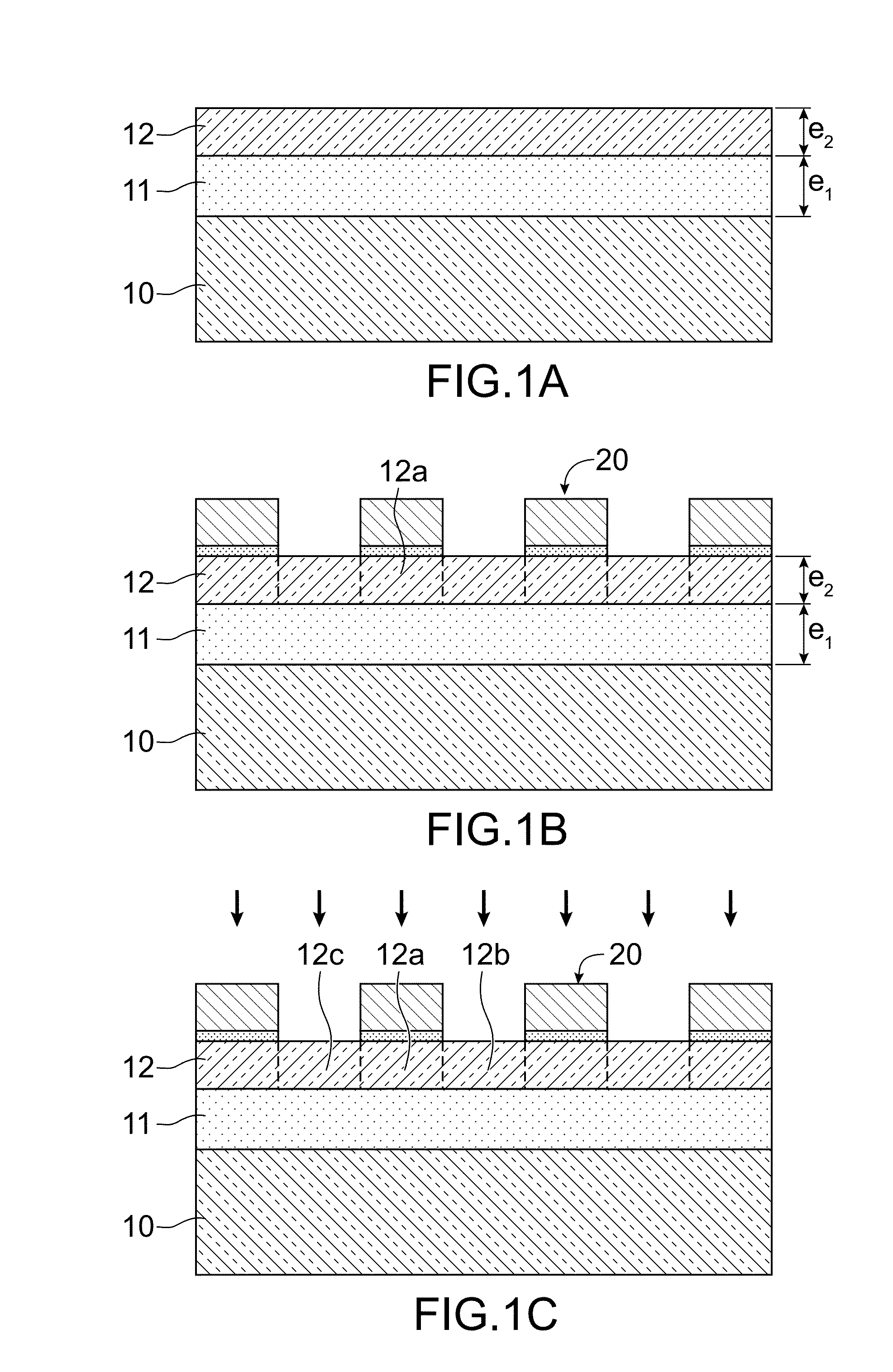
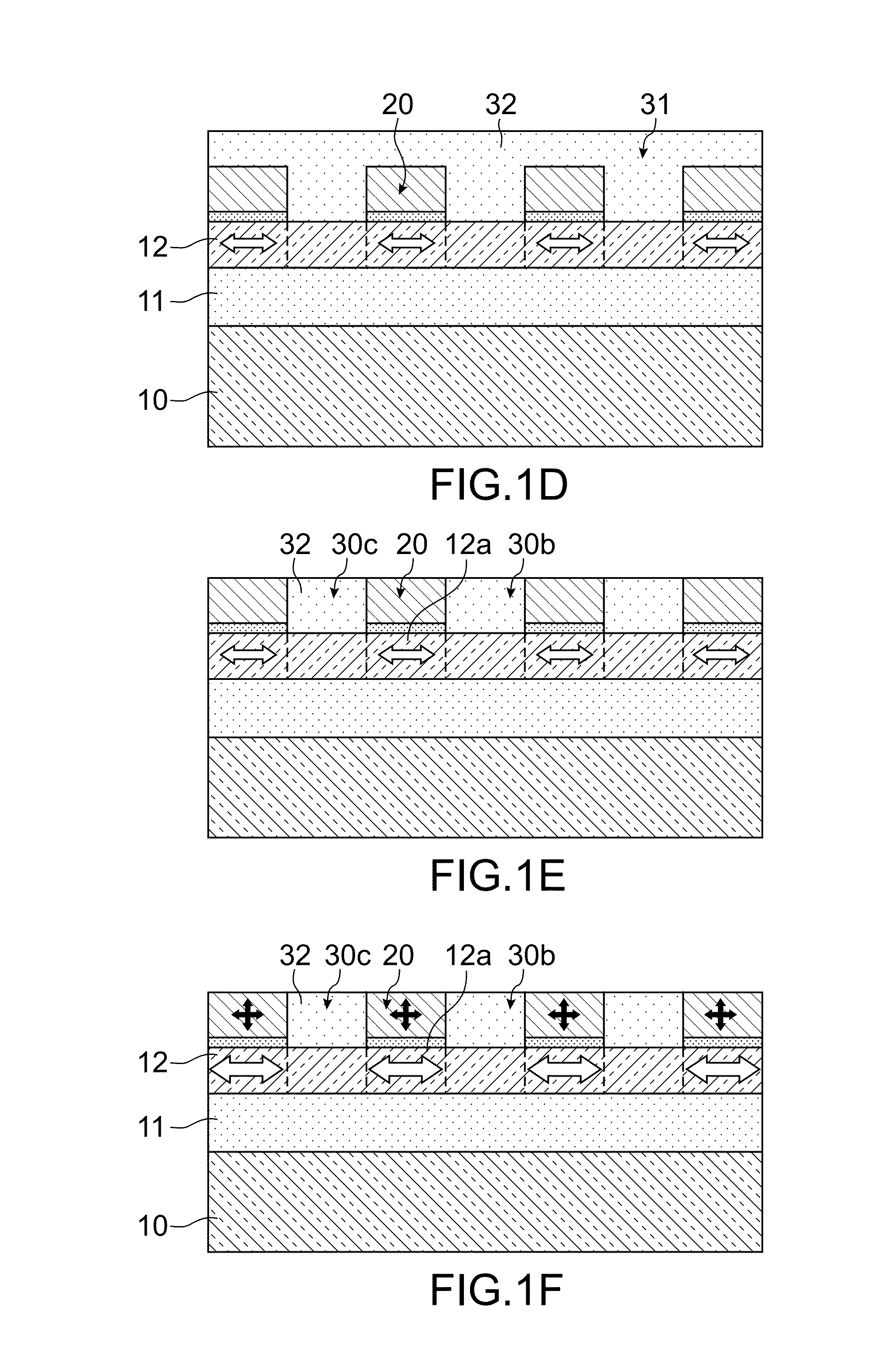
[0045]Identical, similar or equivalent parts of the various figures have the same numeric references to facilitate comparisons between the different figures.

[0046]The various parts shown in the figures are not necessarily all at the same scale to make the figures more easily understandable.

[0047]Furthermore, throughout the following description, terms that depend on the orientation, such as >, >, >, >, > etc. of a structure are applied considering that the structure is oriented as shown on the figures.

DETAILED PRESENTATION OF PARTICULAR EMBODIMENTS

[0048]A first example of the method used to strain at least one semiconducting zone of a transistor channel will now be described with reference to FIGS. 1A-1I and FIG. 7 on which the main steps of this example method are shown.

[0049]The initial material for this method (step E0 in the diagram in FIG. 7) may be a semiconductor on insulator type substrate, for example of the SOI type.

[0050]The substrate thus includes a semiconducting suppor...


PUM


Abstract

Method of straining a transistor channel zone comprising the following steps:
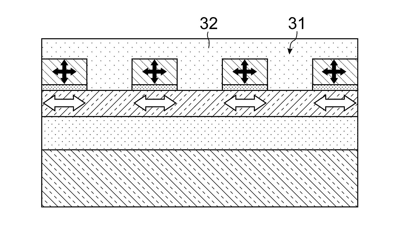
    • a) formation of stress blocks (30b, 30c) arranged so as to induce a given stress in a semiconducting zone (12a),
    • b) form a gate stack on this semiconducting zone (12a) comprising a dielectric material with a high Young's modulus deposited on and in contact with the semiconducting material,
    • c) at least partially remove the stress block(s).

Description

TECHNICAL DOMAIN AND PRIOR ART[0001]This description relates to the domain of transistor structures, and more particularly structures provided with a strained or mechanically strained channel zone.[0002]Mechanical strain means a material for which the crystalline lattice parameter(s) has (have) been extended or shortened.[0003]In the case in which the strained lattice parameter is larger than the so-called “natural” parameter of a crystalline material, the material is said to be strained in tension. When the strained lattice parameter is shorter than the natural lattice parameter, the material is said to be in compressive strain or in compression.[0004]These mechanical strain states are associated with mechanical stress states. As a result, these mechanical strain states are frequently referred to as mechanical stress states. Throughout the remainder of this application, this concept of “strain” will be generically referred to by the term <<stress>>.[0005]A stress applie...

Claims


Application Information

Patent Timeline
IPC IPC(8): H01L29/78H01L29/51H01L29/66
CPCH01L29/7849H01L29/517H01L29/66795H01L29/66545H01L29/7847H01L29/785H01L21/823821H01L29/7851
Inventor REBOH, SHAYMATHIEU, BENOIT
Owner COMMISSARIAT A LENERGIE ATOMIQUE ET AUX ENERGIES ALTERNATIVES
Features
  • Generate Ideas
  • Intellectual Property
  • Life Sciences
  • Materials
  • Tech Scout
  • Unparalleled Data Quality
  • Higher Quality Content
  • 60% Fewer Hallucinations
Learn More