Controlled synthesis of monolithically-integrated graphene structure

a graphene structure and monolithic integration technology, applied in the field of graphene, can solve the problems of high complexity of the silicon microfabrication process, process not meeting the specific materials requirements for fabricating a range of device components based on graphene materials, and the inability to achieve the full potential of graphene as a microfabrication material

Active Publication Date: 2013-08-22
PRESIDENT & FELLOWS OF HARVARD COLLEGE
View PDF3 Cites 40 Cited by
  • Summary
  • Abstract
  • Description
  • Claims
  • Application Information

AI Technical Summary

Benefits of technology

[0010]This graphene circuit configuration and the processes for producing the circuit offer significant advantages over conventional CMOS processes with single-step formation of entire devices and circuits during one graphene synthesis step. In addition, the ability to conduct layer-by-layer assembly of synthesize...

Problems solved by technology

But as the limit of size scaling is approached for such silicon electronics, silicon microfabrication process have become highly complicated; consequently, a demand for the simplification of fabrication processes and the use new materials, beyond silicon, has been rapidly rising for the next generation of circuits.
However, the nature of 1D materials requires assembly and additional integration steps, such as meta...

Method used


Image

  • Controlled synthesis of monolithically-integrated graphene structure
  • Controlled synthesis of monolithically-integrated graphene structure
  • Controlled synthesis of monolithically-integrated graphene structure

Examples


example i

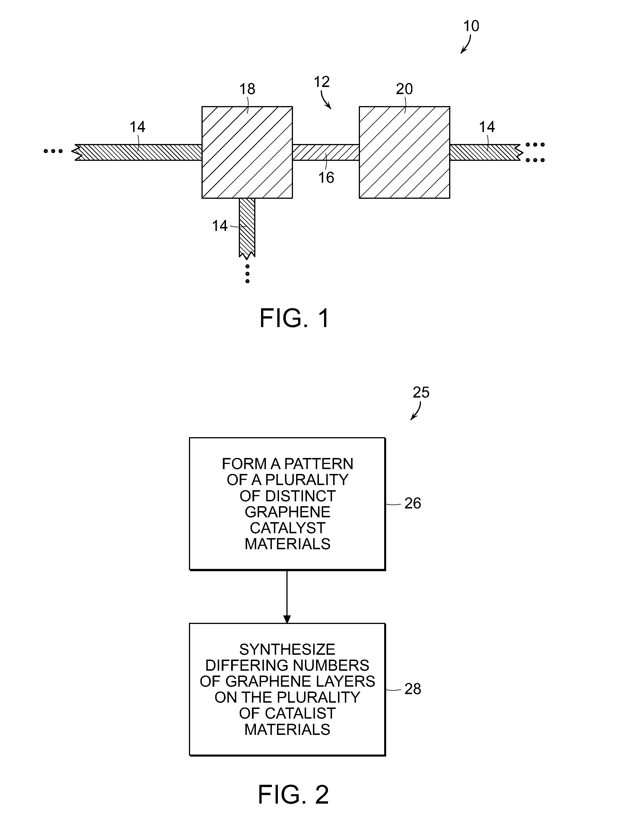
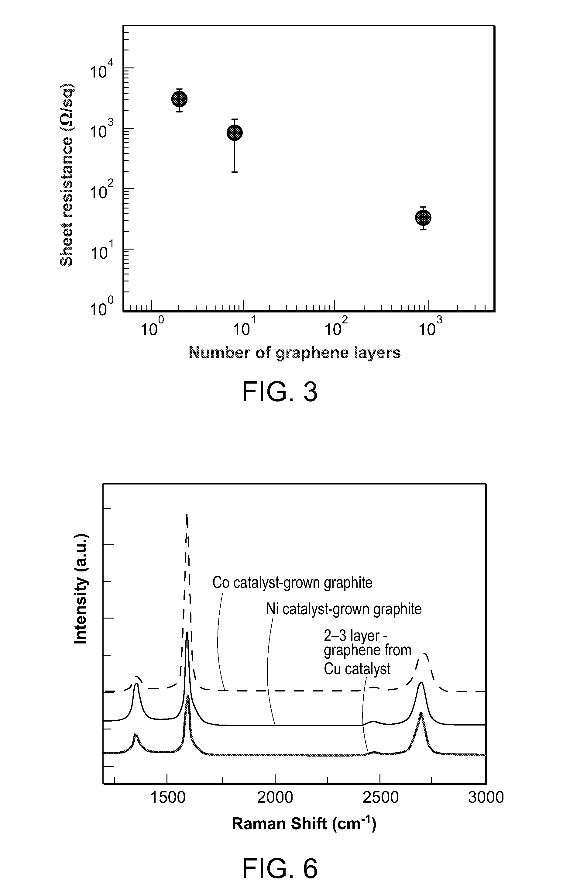
[0058]A geometry of Cu, Ni, and Co graphene catalyst layers was formed for synthesizing differing numbers of graphene layers simultaneously. A silicon fabrication substrate having a top layer of silicon dioxide of about 250 nm in thickness was coated with a film of Cu of 700 nm in thickness having a 5 nm-thick Ni passivation layer to protect against Cu oxidation. Regions of Co of 10 nm, 60 nm, 80 nm, and 120 nm in thickness were patterned and regions of Ni of 20 nm in thickness were patterned in various shapes, all on the Cu / Ni layers. The catalyst structures were subjected to a graphene synthesis step as described above, with the temperature ramped to 1000° C. while the structure was positioned at the edge of the furnace, under the flow of H2 gas at 1200 sccm and Ar gas at 500 sccm. When the furnace reached the graphene synthesis temperature, the substrate was quickly moved to the center of the heating zone. CVD synthesis of the graphene materials was then be carried out under cond...

example ii

[0064]Following the graphene synthesis process of Example I, a graphene catalyst region of Cu of 700 nm in thickness having a 5 nm-thick Ni top layer and a graphene catalyst region of a layered combination of Cu / Ni / Co of thicknesses 700 nm / 5 nm / 400 nm was subjected to the synthesis process of Example I. With the PMMA handle layer transfer procedure of Example I, the resulting graphene and graphite structures were transferred to a layer of 285 nm-thick silicon dioxide on a silicon wafer, and the structures were plasma etched with an oxygen plasma to produce channel regions. Electrodes were then deposited as 70 nm-thick Au regions, with a 3 nm-thick Cr adhesion layer. FIG. 9A is a schematic of this arrangement, with a channel 70 between a source, S, and drain, D, on the oxide layer 72 and substrate 74. The Cu / Ni catalyst region produced a graphene region of 2-3 layers and the Cu / Ni / Co catalyst region produced a region of about 850 layers of graphene.

[0065]FIG. 9B is a plot of current ...

example iii

[0066]A back-gated graphene FET like that of FIG. 4F was fabricated following the synthesis process of Examples I and II. A catalyst pattern like that of FIG. 4D was employed, with a blanket coating of Cu of 700 nm in thickness / Ni of 5 nm thickness, for producing a 2-3 layer graphene transistor channel, and regions of Cu of 700 nm in thickness / Ni of 5 nm in thickness / Co of 400 nm in thickness, for producing graphite source (S) and drain (D) transistor regions. After CVD synthesis of the graphene and graphite device regions following the process of Example I, the structure was transferred to a 285 nm-thick SiO2 dielectric layer on a Si wafer after a reactive ion etch (RIE) isolation step, to produce backgate monolithic graphene transistors with graphite S / D regions. The FET channel region was etched to provide dimensions of 1 μm in width and 5 μm in length.

[0067]The current, ID, as a function of backgate voltage, VG, with the silicon substrate biased as the backgate, was measured at ...


PUM


Abstract

In a method for fabricating a graphene structure, there is formed on a fabrication substrate a pattern of a plurality of distinct graphene catalyst materials. In one graphene synthesis step, different numbers of graphene layers are formed on the catalyst materials in the formed pattern. In a method for fabricating a graphene transistor, on a fabrication substrate at least one graphene catalyst material is provided at a substrate region specified for synthesizing a graphene transistor channel and at least one graphene catalyst material is provided at a substrate region specified for synthesizing a graphene transistor source, and at a substrate region specified for synthesizing a graphene transistor drain. Then in one graphene synthesis step, at least one layer of graphene is formed at the substrate region for the graphene transistor channel, and at the regions for the transistor source and drain there are formed a plurality of layers of graphene.

Description

CROSS-REFERENCE TO RELATED APPLICATIONS[0001]This application claims the benefit of U.S. Provisional Application No. 61 / 3807672, filed Sep. 8, 2010, the entirety of which is hereby incorporated by reference.STATEMENT REGARDING FEDERALLY SPONSORED RESEARCH[0002]This invention was made with government support under Contract USGC 15095320-HA awarded by the U.S. Central Intelligence Agency and under Contract N00244-09-1-0078-DOD35CAP awarded by U.S. Department of Defense. The Government has certain rights in the invention.BACKGROUND[0003]This invention relates generally to graphene, and more particularly relates to graphene synthesis.[0004]Over the past four decades, a reduction in the size of silicon metal-oxide-semiconductor field effect transistors (MOSFETs) has been one key to the progress that has been achieved in producing advanced microfabricated, integrated electronics. But as the limit of size scaling is approached for such silicon electronics, silicon microfabrication process ...

Claims


Application Information

Patent Timeline
IPC IPC(8): H01L21/02H01L29/66H01L29/786
CPCB82Y30/00H01L2924/0002C01B31/0453H01L21/02381H01L21/02488H01L21/02491H01L21/02494H01L21/02502H01L21/02527H01L21/0262H01L21/02645H01L21/02664H01L23/53276H01L29/1606H01L29/66742H01L29/7781H01L29/78618H01L29/78684H01L29/66477B82Y40/00H01L2924/00C01B32/186Y10S977/734Y10S977/936Y10S977/938
Inventor PARK, JANG-UNGNAM, SUNGWOOLIEBER, CHARLES M.
Owner PRESIDENT & FELLOWS OF HARVARD COLLEGE
Why Eureka
Try Eureka