Complementary field-effect transistors having enhanced performance with a single capping layer

a field-effect transistor and enhanced performance technology, applied in the field of field-effect transistors, can solve the problems of difficulty in enhancing the performance of both n-channel and p-channel devices simultaneously, and achieve the effect of enhancing their performan

Inactive Publication Date: 2006-12-21
RGT UNIV OF CALIFORNIA
View PDF6 Cites 40 Cited by
  • Summary
  • Abstract
  • Description
  • Claims
  • Application Information

AI Technical Summary

Benefits of technology

[0005] In accordance with the invention, a stressed film or capping layer is formed over the source, gate stack (comprising the channel, gate dielectric layer or layers, and the gate electrode layer or layers), and drain regions of both n-channel and p-channel MOSFETs in a CMOS device to enhance their performance.
[0006] More particularly, in one embodiment, the NMOS transistor is fabricated in silicon having a (100) surface crystalline orientation, and the PMOS transistor is fabricated in silicon having a (110) surface crystalline orientation. Such a combination of surface crystalline orientations can be realized in a hybrid substrate having multiple layers of silicon with planes of different crystallographic orientation or by simple rotation of the layouts of vertical transistors formed from a single layer of silicon. For a (100) surface crystalline orientation, a tensile film or capping layer can induce tensile stress in the transistor channel region, which improves electron mobility in the stressed silicon. Conversely, for a (110) surface crystalline orientation, a tensile film or capping layer can induce compressive stress in the transistor channel region which improves hole mobility in the stressed silicon.

Problems solved by technology

However, it is difficult to enhance the performance of both n-channel and p-channel devices simultaneously, because tensile stress is required in the n-channel MOSFET channel, whereas uniaxial compressive stress is required in the p-channel MOSFET channel, to enhance carrier mobility.

Method used


Image

  • Complementary field-effect transistors having enhanced performance with a single capping layer
  • Complementary field-effect transistors having enhanced performance with a single capping layer
  • Complementary field-effect transistors having enhanced performance with a single capping layer

Examples


Embodiment Construction

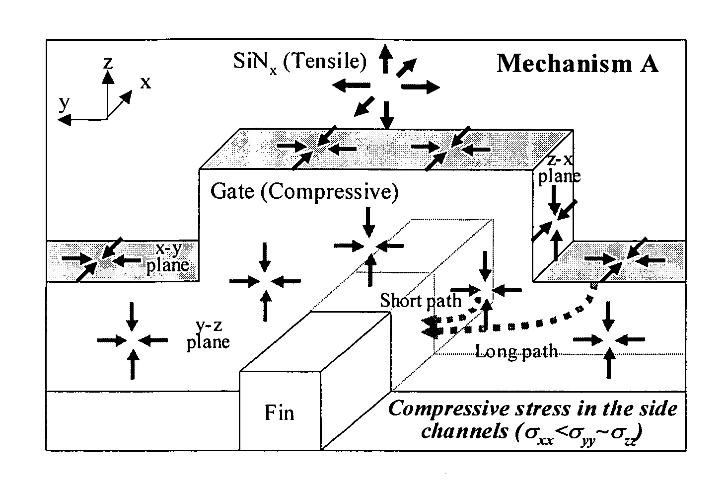
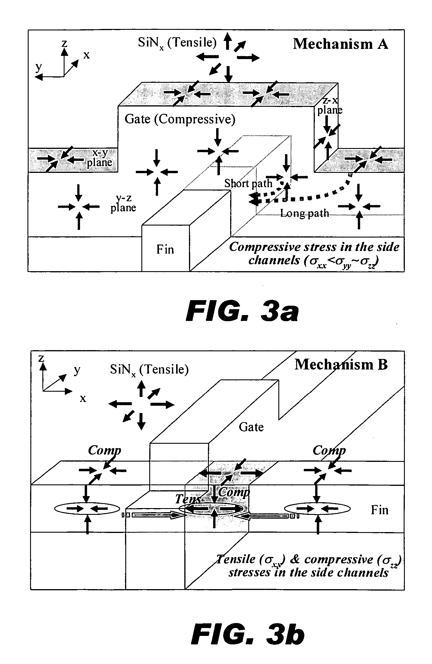
[0016] The present invention can be implemented with a single sequence of manufacturing process steps to enhance performance in both n-channel MOSFETs and p-channel MOSFETs in a CMOS device. In one embodiment, the n-channel transistors have (100) channel surface crystalline orientation, and the p-channel transistors have (110) channel surface crystalline orientation. A tensile film or capping layer overlying the source, gate stack, and drain regions of the transistors will then induce tensile stress in the channel of (100) n-channel transistors and will induce compressive stress in the channel of (110) p-channel transistors, which respectively enhances the mobilities of electrons and holes in the n-channel and the p-channel MOSFETs.

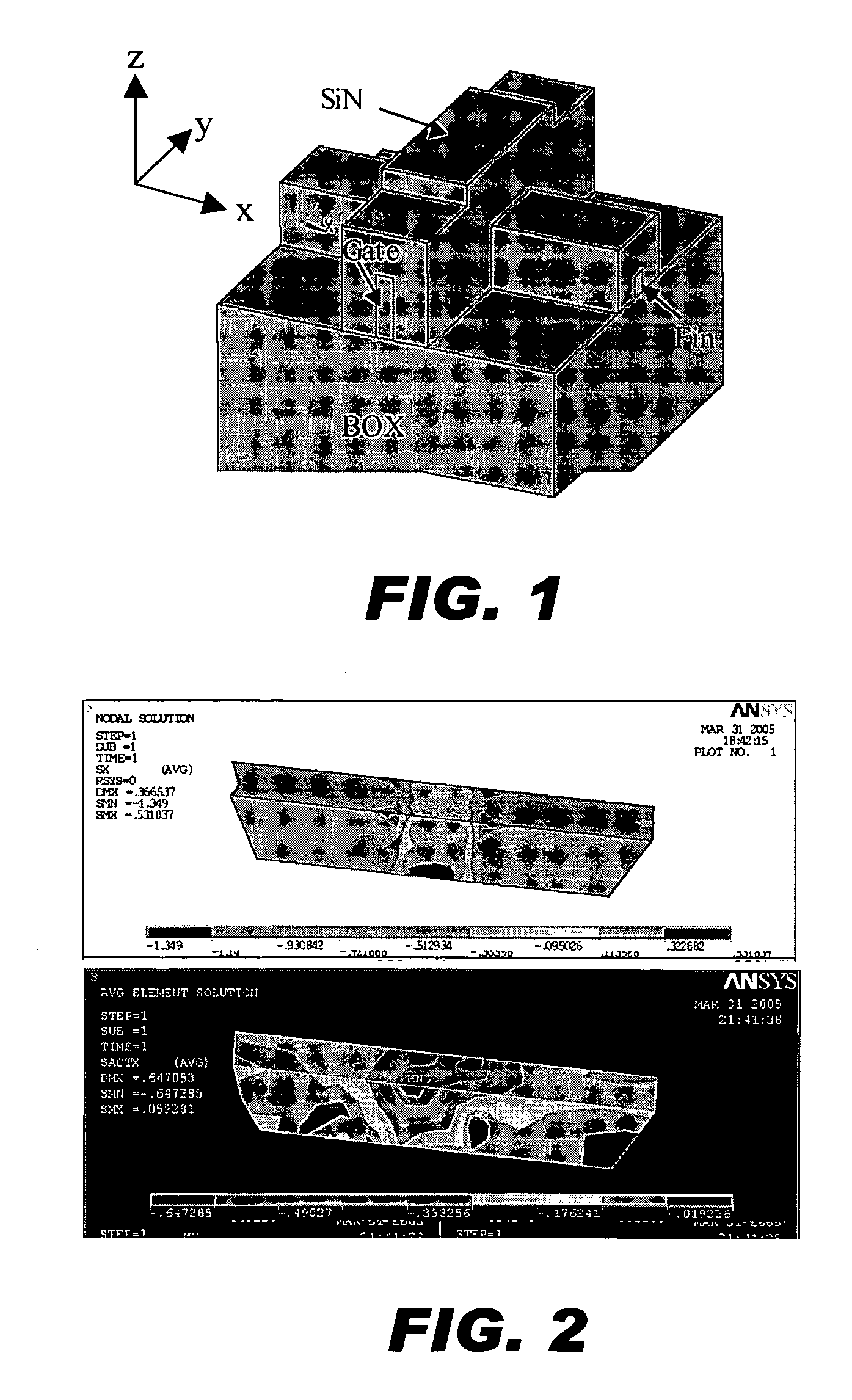
[0017]FIG. 1 is a perspective view of a FinFET transistor in which the invention can be practiced. As described in detail in U.S. Pat. No. 6,413,802, supra, the source, S, and the drain, D, are connected by a fin-shaped channel with a gate electrode, G, ...


PUM


Abstract

Performance of a complementary metal-oxide-semiconductor (CMOS) device having n-channel MOS transistors and p-channel MOS transistors is enhanced by providing a single capping layer overlying the MOS transistors with the single capping layer inducing stress in the transistor channel regions to enhance carrier mobility. The n-channel transistor is preferably fabricated in silicon having a (100) crystalline channel surface orientation, and the p-channel transistor is preferably fabricated in silicon having a (110) channel surface crystalline orientation. A tensile stress in the single capping layer induces tensile stress in the channel of the (100) n-channel transistor thereby enhancing the mobility of electrons while tensile stress in the single capping layer induces compressive stress in the channel of the (110) p-channel transistor thereby enhancing the mobility of holes. Alternatively, the n-channel transistor is fabricated in silicon having a (110) crystalline channel surface orientation, and the p-channel transistor is fabricated in silicon having a (100) channel surface crystalline orientation. A compressive stress in the single capping layer induces tensile stress in the channel of the (110) n-channel transistor thereby enhancing the mobility of electrons while compressive stress in the single capping layer induces compressive stress in the channel of the (100) p-channel transistor thereby enhancing the mobility of holes.

Description

BACKGROUND OF THE INVENTION [0001] This invention relates generally to field effect transistors (FETs), and more particularly the invention relates to use of a stressed capping layer to enhance the performance of complementary metal-oxide-semiconductor (CMOS) integrated-circuit (IC) devices. [0002] CMOS IC devices comprise n-channel (NMOS) and p-channel (PMOS) transistors which toggle on-off in a complementary fashion in response to input voltage signals. The transistors can have a planar structure, in which the surfaces of the source, channel, and drain regions are substantially located in a single plane, as in a conventional bulk-silicon (bulk-Si) MOSFET or silicon-on-insulator (SOI) MOSFET, or the transistors can have a vertical structure such as in the double gate FinFET structure as described in U.S. Pat. No. 6,413,802. [0003] Transistor performance depends on mobile carrier (hole or electron) mobility. Strained-silicon technologies have been widely investigated to enhance the ...

Claims


Application Information

Patent Timeline
Patent Type & Authority Applications(United States)
IPC IPC(8): H01L21/336
CPCH01L21/823807H01L21/823821H01L21/823864H01L29/785H01L29/045H01L29/66795H01L29/7843H01L21/845
Inventor SHIN, KYOUNGSUBKING, TSU-JAE
Owner RGT UNIV OF CALIFORNIA
Why Eureka
Try Eureka