In-situ nitride/oxynitride processing with reduced deposition surface pattern sensitivity

a technology of oxide deposition layer, which is applied in the direction of semiconductor devices, semiconductor/solid-state device details, electrical apparatus, etc., can solve the problems of exacerbated instability and undesirable thickness dependence of deposited dielectric layer upon, and achieve enhanced drive current, reduced oxide deposition surface pattern sensitivity, and enhanced drive current

Active Publication Date: 2006-03-07
INNOVATIVE FOUNDRY TECH LLC
View PDF7 Cites 43 Cited by
  • Summary
  • Abstract
  • Description
  • Claims
  • Application Information

AI Technical Summary

Benefits of technology

[0008]An advantage of the present invention is a method of fabricating a semiconductor device comprising transistors with enhanced drive currents.
[0009]Another advantage of the present invention is a method of fabricating a semiconductor device with reduced oxide deposition surface pattern sensitivity.
[0010]Another advantage of the present invention is a semiconductor device comprising transistors with enhanced drive currents.
[0011]Additional advantages and other aspects and features of the present invention will be set forth in the description which follows and in part will become apparent to those having ordinary skill in the art upon examination of the following or may be learned from the practice of the present invention. The advantages of the present invention may be realized and obtained as particularly pointed out in the appended claims.
[0012]According to the present invention, the foregoing and other advantages are obtained in part by a semiconductor device comprising: A substrate; a plurality of transistors formed on the substrate, each transistor comprising source/drain regions and a gate electro

Problems solved by technology

Accordingly, in conventional CMOS transistors, the drive current of the PMOS transistor is less than the drive current of the NMOS transistor creating an imbalance.
This imbalance is exacerbated in CMOS transistors fabricated on or within a tensilely stressed active device area formed in a

Method used


Image

  • In-situ nitride/oxynitride processing with reduced deposition surface pattern sensitivity
  • In-situ nitride/oxynitride processing with reduced deposition surface pattern sensitivity
  • In-situ nitride/oxynitride processing with reduced deposition surface pattern sensitivity

Examples


Embodiment Construction

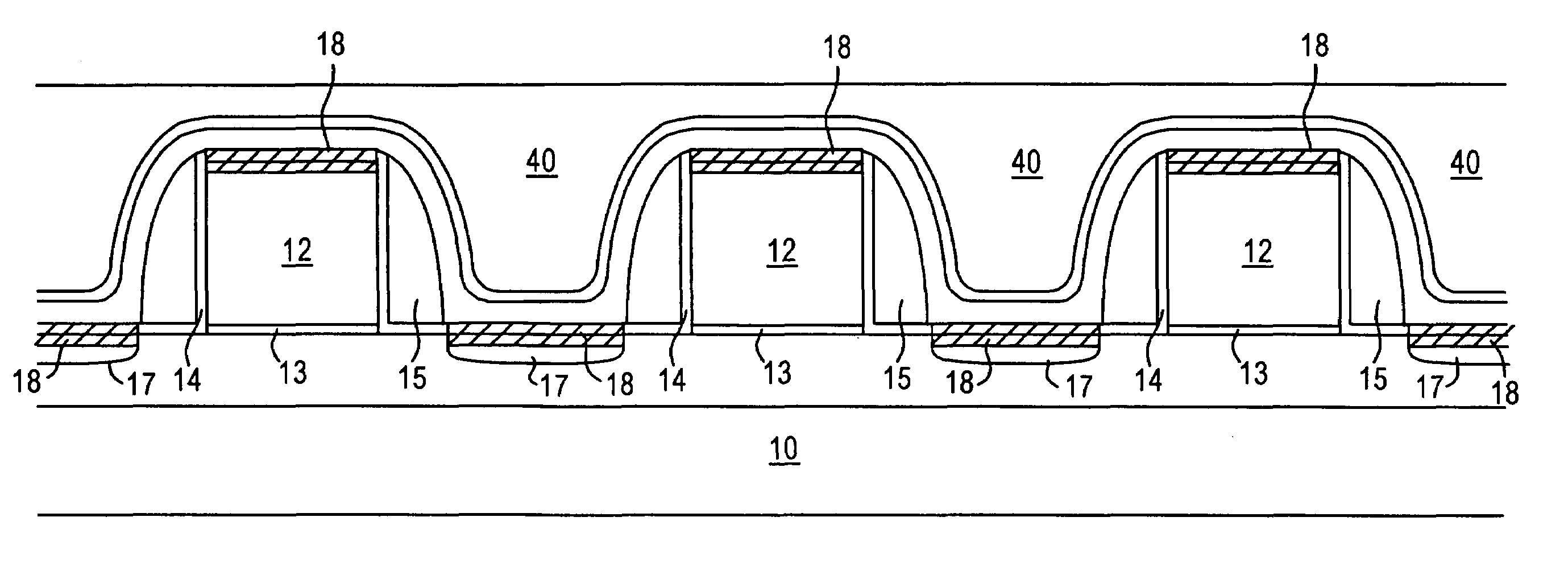
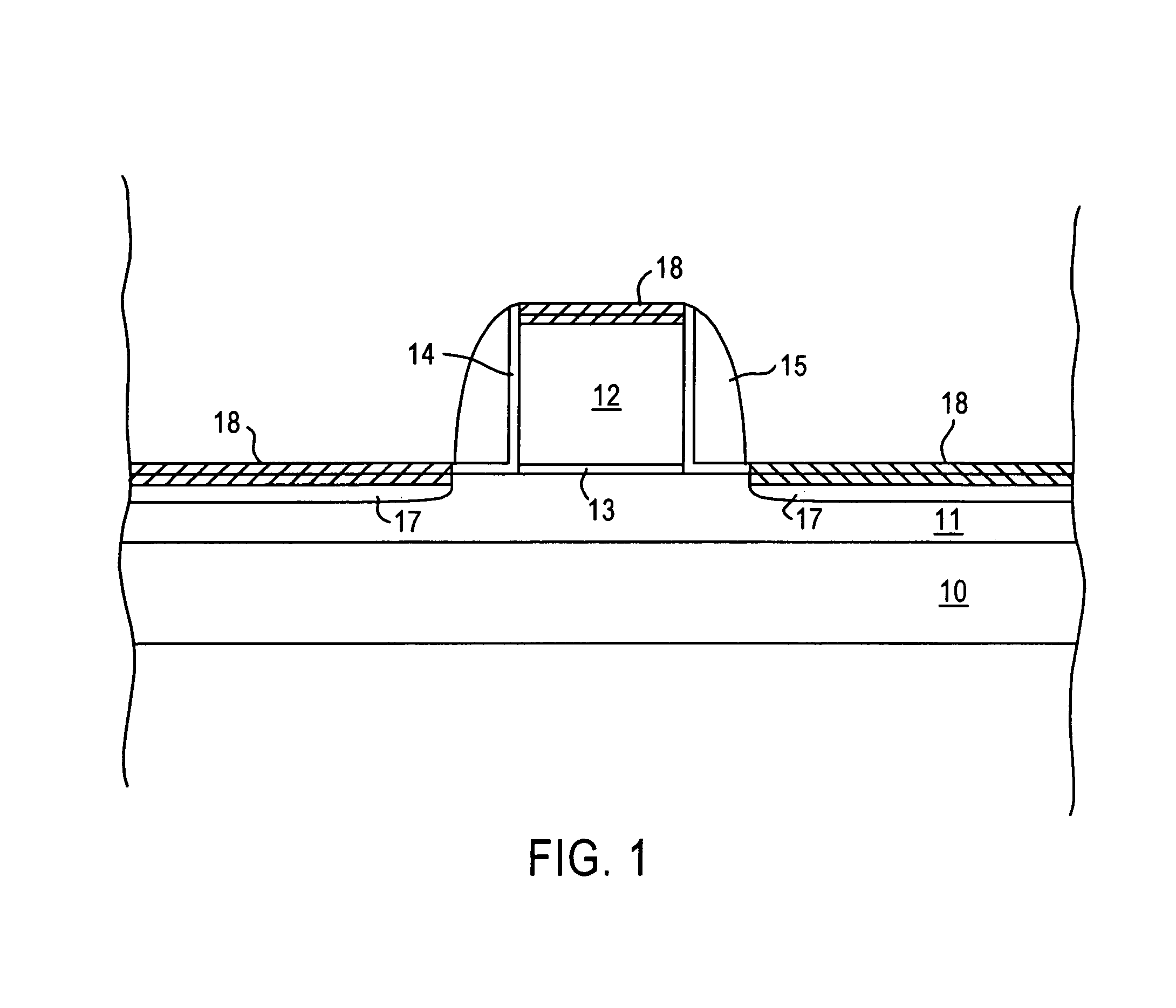
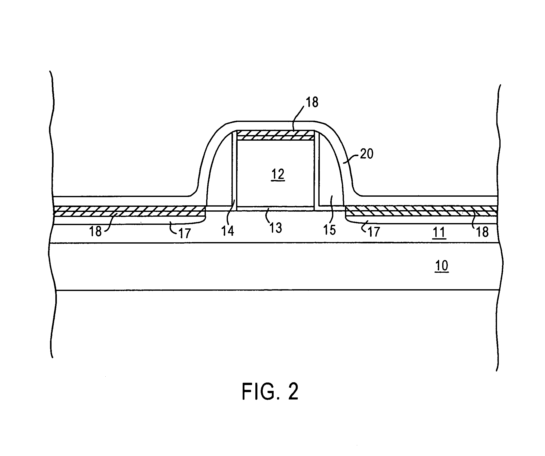
[0019]The present invention addresses and solves the problem of increasing the drive current of transistors, including transistors based on strained Si / Si—Ge substrates, in a cost effective and efficient manner by significantly enhancing channel carrier mobility. The present invention also addresses and solves the loading problem wherein the thickness of a deposited dielectric layer depends upon differences between topographical features, as between closely spaced gate electrodes and isolated electrodes. The present invention stems in part, from the recognition that the channel carrier mobility of transistors, particularly transistors based on strained Si / Si—Ge substrates, can be increased by applying a stress thereto. The present invention also stems, in part, from the recognition that the surface pattern sensitivity of a dielectric layer during deposition, as when depositing silicon oxide layer by SACVD, can be eliminated or significantly reduced by forming a transition layer of s...


PUM


Abstract

Carrier mobility in transistor channel regions is increased by depositing a conformal stressed liner. Embodiments include forming a silicon oxynitride layer on the stressed liner to reduce or eliminate deposition surface pattern sensitivity during gap filling, and in-situ SACVD of silicon oxide gap fill directly on the stressed liner with reduced pattern sensitivity. Embodiments also include the use of Si—Ge substrates.

Description

FIELD OF THE INVENTION[0001]The present invention relates to the fabrication micro-miniaturized semiconductor devices comprising transistors exhibition enhanced channel carrier mobility. The present invention is particularly applicable in fabricating high speed transistors efficient, simplified methodology with reduced or no deposition surface pattern sensitivity during gap fill deposition.BACKGROUND OF THE INVENTION[0002]The relentless pursuit of miniaturized, high speed semiconductor devices continues to challenge the limitations of conventional semiconductor materials and fabrication techniques. Conventional semiconductor devices typically comprise a plurality of active devices in or on a common semiconductor substrate, e.g., CMOS devices comprising at least a pair of PMOS and NMOS transistors in spaced adjacency. Current technology utilizes crystalline semiconductor wafers as substrates, such as a lightly p-doped epitaxial (“epi”) layer of silicon (Si) grown on a heavily-doped, ...

Claims


Application Information

Patent Timeline
IPC IPC(8): H01L29/78
CPCH01L21/3145H01L21/76829H01L29/7843H01L21/76832Y10S257/90H01L21/02274H01L21/02211H01L21/02164H01L21/0214H01L21/022H01L21/0217
Inventor SUN, SEY-PING
Owner INNOVATIVE FOUNDRY TECH LLC
Why Eureka
Try Eureka