Image sensor with transfer gate having multiple channel sub-regions

a technology of image sensor and transfer gate, which is applied in the field of image sensor, can solve the problems of excess charge spilling into adjacent photosensitive elements, and the conventional transfer gate often suffers from image lag and blooming

Inactive Publication Date: 2011-02-10
OMNIVISION TECH INC
View PDF9 Cites 40 Cited by
  • Summary
  • Abstract
  • Description
  • Claims
  • Application Information

AI Technical Summary

Problems solved by technology

However, conventional transfer gates often suffer from image lag and blooming.
Image lag may result from the conventional conducting channel region being unable to remove all the signal from the photosensitive element such that a residual signal remains during successive readings of the pixel.
Blooming may result from the photosensitive element converting high intensity portions of an image which may cause excess charge to spill into adjacent photosensitive elements.
Blooming may limit the imaging sensor's dynamic range and may limit the types of commercial applications of the imaging sensor.

Method used


Image

  • Image sensor with transfer gate having multiple channel sub-regions
  • Image sensor with transfer gate having multiple channel sub-regions
  • Image sensor with transfer gate having multiple channel sub-regions

Examples


Embodiment Construction

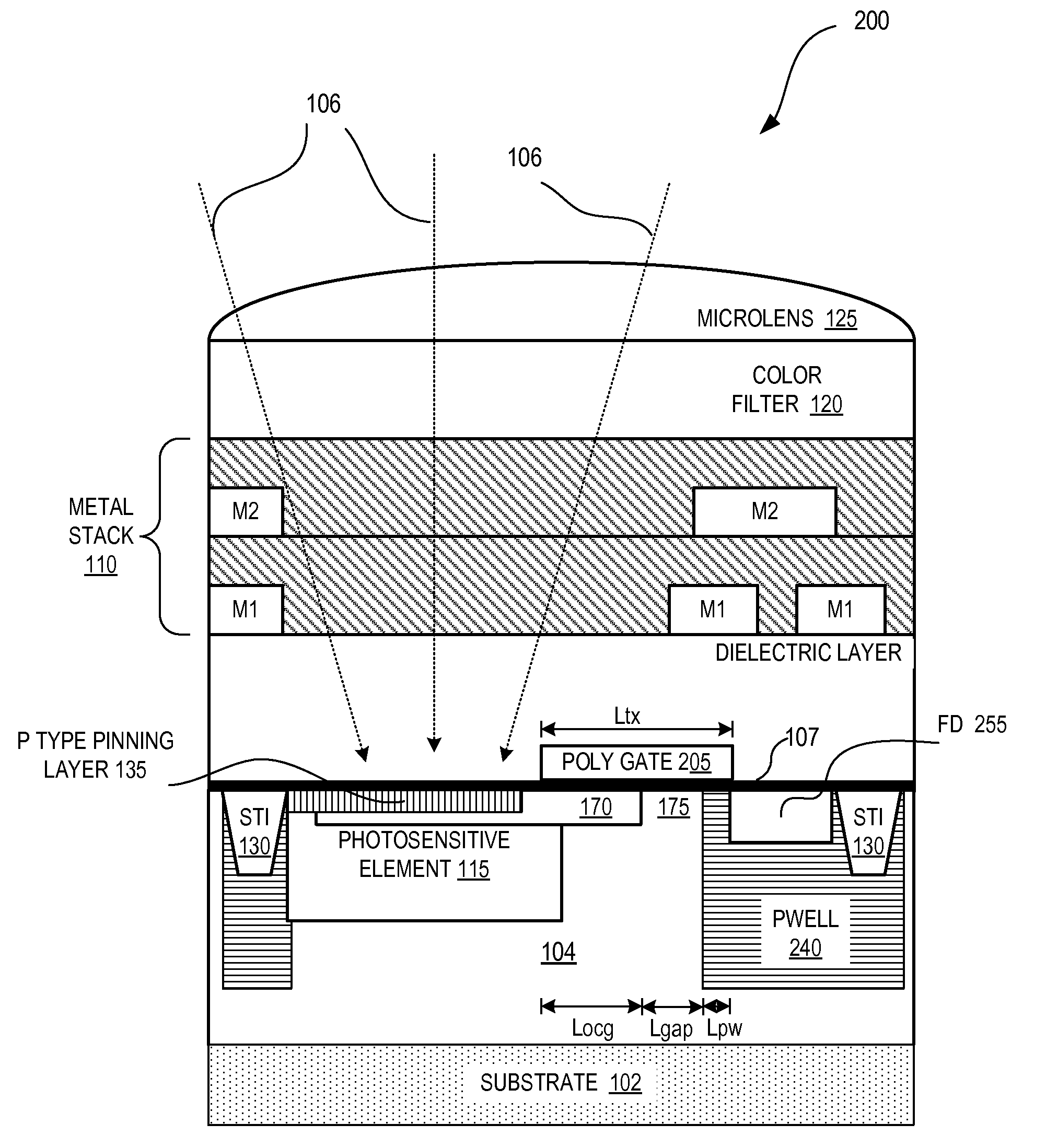
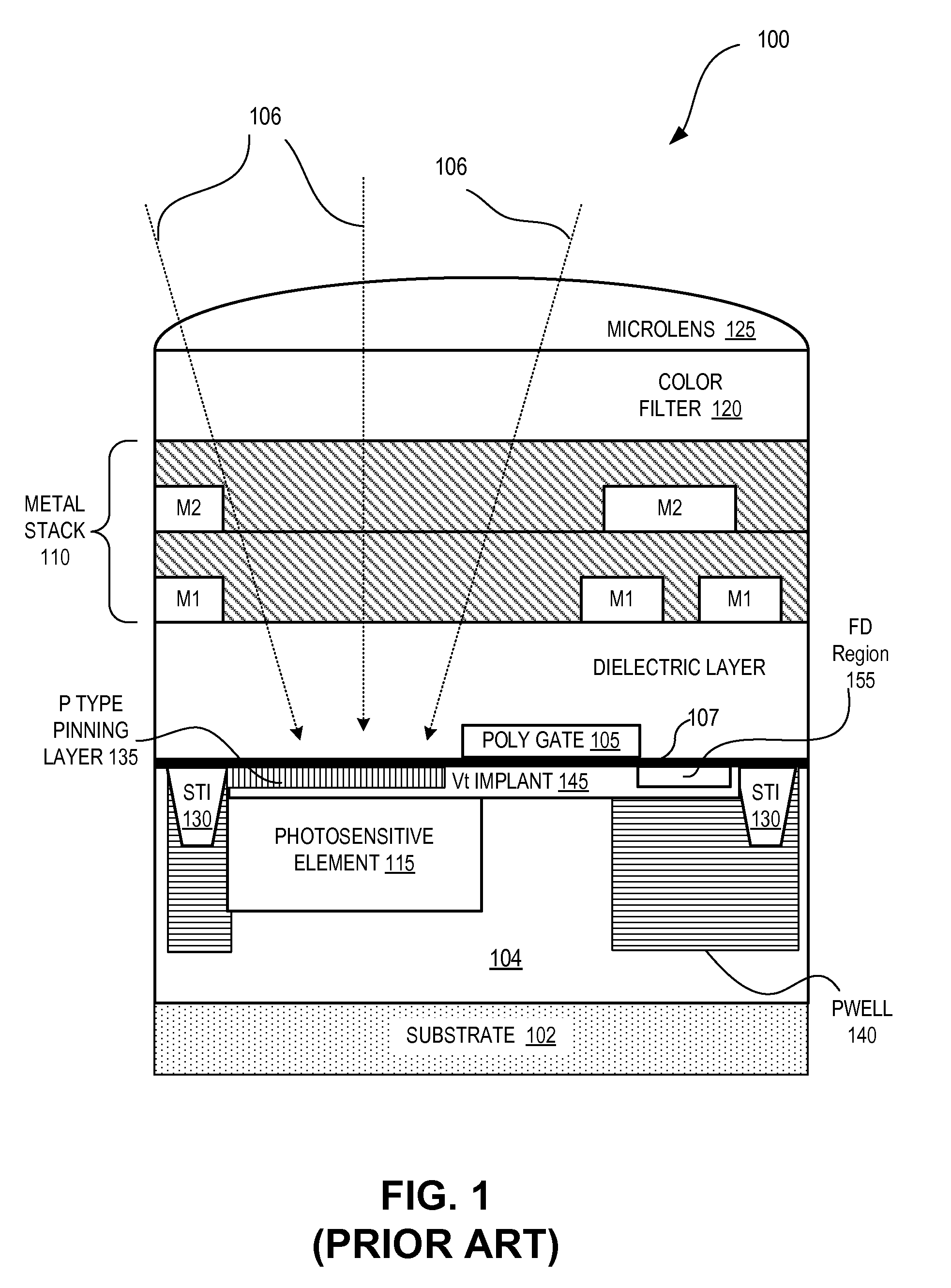
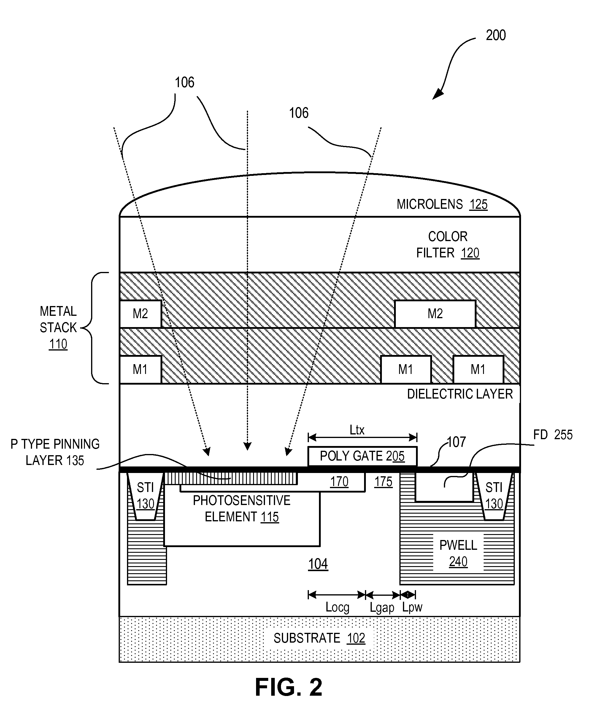
[0014]Embodiments of a pixel, an image sensor, an imaging system, and methods of fabrication of a pixel, image sensor, and imaging system having improved image lag and blooming characteristics are described herein. In the following description numerous specific details are set forth to provide a thorough understanding of the embodiments. One skilled in the relevant art will recognize, however, that the techniques described herein can be practiced without one or more of the specific details, or with other methods, components, materials, etc. In other instances, well-known structures, materials, or operations are not shown or described in detail to avoid obscuring certain aspects. For example, although not illustrated, it should be appreciated that image sensor pixels may include a number of conventional layers (e.g., antireflective films, etc.) used for fabricating CIS pixels. Furthermore, the illustrated cross sections of image sensor pixels illustrated herein do not necessarily ill...


PUM


Abstract

An image sensor pixel includes a photosensitive element, a floating diffusion region and a transfer transistor channel region. The transfer transistor channel region is disposed between the photosensitive region and the floating diffusion region. The transfer transistor channel region includes a first channel sub-region having a first doping concentration and a second channel sub-region having a second doping concentration that is different from the first doping concentration.

Description

REFERENCE TO PRIOR APPLICATIONS[0001]This application claims the benefit of U.S. Provisional Application No. 61 / 232,369, filed Aug. 7, 2009, hereby incorporated by reference.TECHNICAL FIELD[0002]This disclosure relates generally to image sensors, and in particular but not exclusively, relates to CMOS image sensors.BACKGROUND INFORMATION[0003]Image sensors are widely used in digital still cameras, cellular phones, security cameras, as well as in, medical, automobile, and other applications. Complementary metal-oxide-semiconductor (“CMOS”) technology is used to manufacture lower cost image sensors on silicon substrates. In a large number of image sensors, the image sensor commonly includes several light sensor cells or pixels. A typical individual pixel includes a micro-lens, a filter, a photosensitive element, a floating diffusion region, and one or more transistors for reading out a signal from the photosensitive element. One of the transistors included in the pixel is commonly refe...

Claims


Application Information

Patent Timeline
Patent Type & Authority Applications(United States)
IPC IPC(8): H04N5/335H01L31/18
CPCH01L27/14616H01L27/14603
Inventor NOZAKI, HIDETOSHIDAI, TIEJUN
Owner OMNIVISION TECH INC
Why Eureka
Try Eureka