Method and structure for controlling stress in a transistor channel

a transistor channel and stress control technology, applied in the direction of semiconductor devices, electrical appliances, basic electric elements, etc., can solve the problem that the performance of the pfet is generally disadvantageous to the benefit of the nfet performan

Active Publication Date: 2005-07-21
TAIWAN SEMICON MFG CO LTD
View PDF2 Cites 39 Cited by
  • Summary
  • Abstract
  • Description
  • Claims
  • Application Information

AI Technical Summary

Problems solved by technology

That is, because the type of stress which is beneficial for the performanc

Method used


Image

  • Method and structure for controlling stress in a transistor channel
  • Method and structure for controlling stress in a transistor channel
  • Method and structure for controlling stress in a transistor channel

Examples


Embodiment Construction

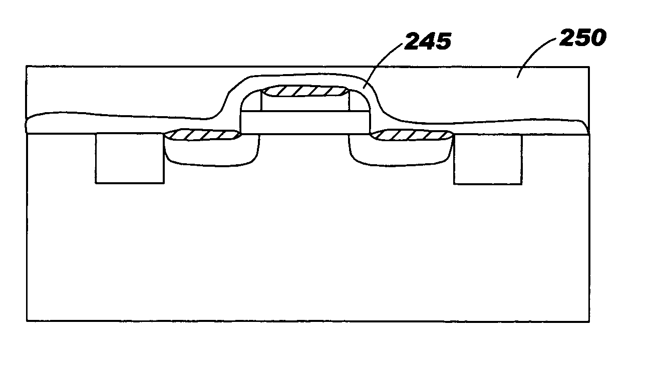
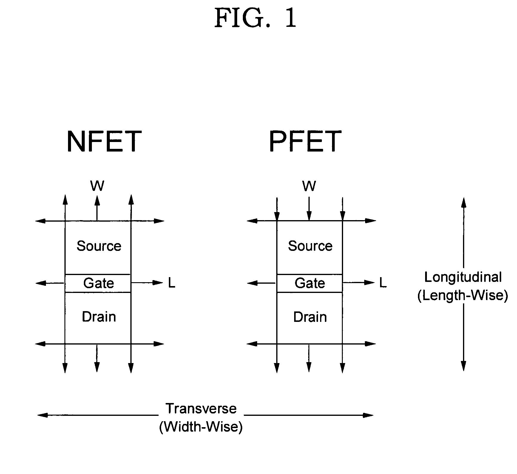
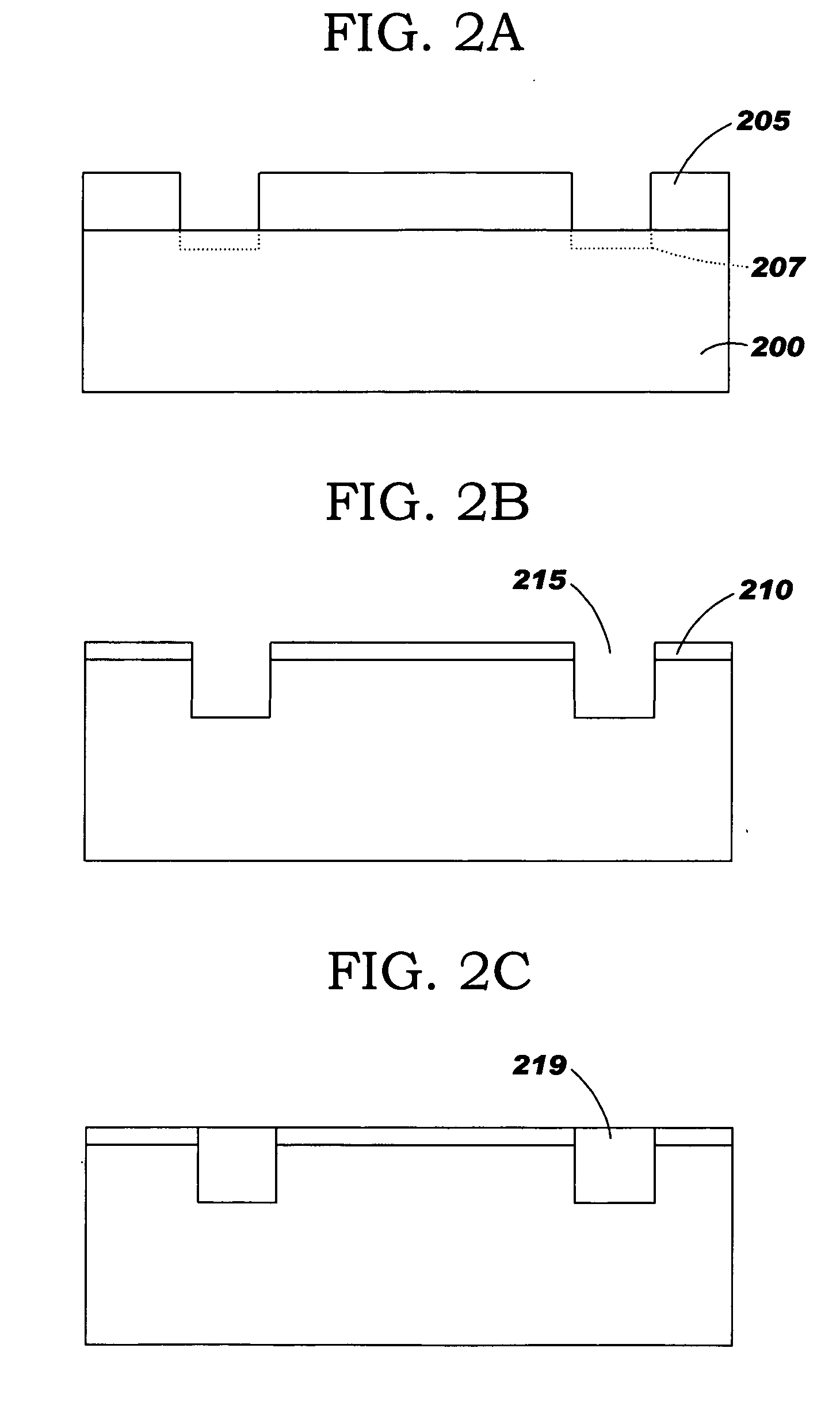
[0018] The invention provides a method for fabricating devices with improved performance characteristics. Tensile and / or compressive stresses can be provided in the channel of a transistor depending on the proximity of the grown stress / strain layer to the channel of the transistor. In an aspect of this invention, by selectively adjusting the topography of the shallow-trench-isolation oxide, which generally surrounds the transistor, tensile stresses can be provided in the channel of NFETs and compressive stresses can be provided in the channel of PFETs such that the performance of both the NFETs and the PFETs can be improved using the same stress / strain layer.

[0019] In this invention, a stress layer, such as a SiGe layer, for example, is used to form stresses in a channel of the semiconductor device. When a SiGe layer is grown on a semiconductor layer the surrounding semiconductor material is subjected to tensile stress while the grown SiGe layer is subjected to compressive stress. ...


PUM


Abstract

A method for manufacturing a device including an n-type device and a p-type device. In an aspect of the invention, the method involves forming a shallow-trench-isolation oxide (STI) isolating the n-type device from the p-type device. The method further involves adjusting the shallow-trench-isolation oxide corresponding to at least one of the n-type device and the p-type device such that a thickness of the shallow-trench-isolation oxide adjacent to the n-type device is different from a thickness of the shallow-trench-isolation oxide adjacent to the p-type device, and forming a strain layer over the semiconductor substrate.

Description

BACKGROUND OF INVENTION [0001] The invention generally relates to methods for manufacturing a semiconductor device with improved device performance, and more particularly to methods for manufacturing semiconductor devices which impose tensile and compressive stresses in the substrate of the device during device fabrication. [0002] Generally, metal-oxide semiconductor transistors include a substrate made of a semiconductor material, such as silicon. The transistors typically include a source region, a channel region and a drain region within the substrate. The channel region is located between the source and the drain regions. A gate stack, which usually includes a conductive material, a gate oxide layer and sidewall spacers, is generally provided above the channel region. More particularly, the gate oxide layer is typically provided on the substrate over the channel region, while the gate conductor is usually provided above the gate oxide layer. The sidewall spacers help protect the...

Claims


Application Information

Patent Timeline
IPC IPC(8): H01L21/336H01L21/762H01L21/8238
CPCH01L21/76229H01L21/823807H01L21/823878H01L29/7842H01L29/6656H01L29/66575H01L29/665H01L29/7846
Inventor YANG, HAINING S.ZHU, HUILONG
Owner TAIWAN SEMICON MFG CO LTD
Why Eureka
Try Eureka