

Semiconductor device and manufacturing method thereof
a semiconductor and semiconductor technology, applied in the direction of optics, transistors, instruments, etc., can solve the problems of reducing the precision of alignment in the photolithography step, the size of the substrate becomes distorted, and the effect of being easily effected by bending and warping
- Summary
- Abstract
- Description
- Claims
- Application Information
AI Technical Summary
Benefits of technology
Problems solved by technology
Method used
Image

Examples
embodiment mode 1
(Embodiment Mode 1)
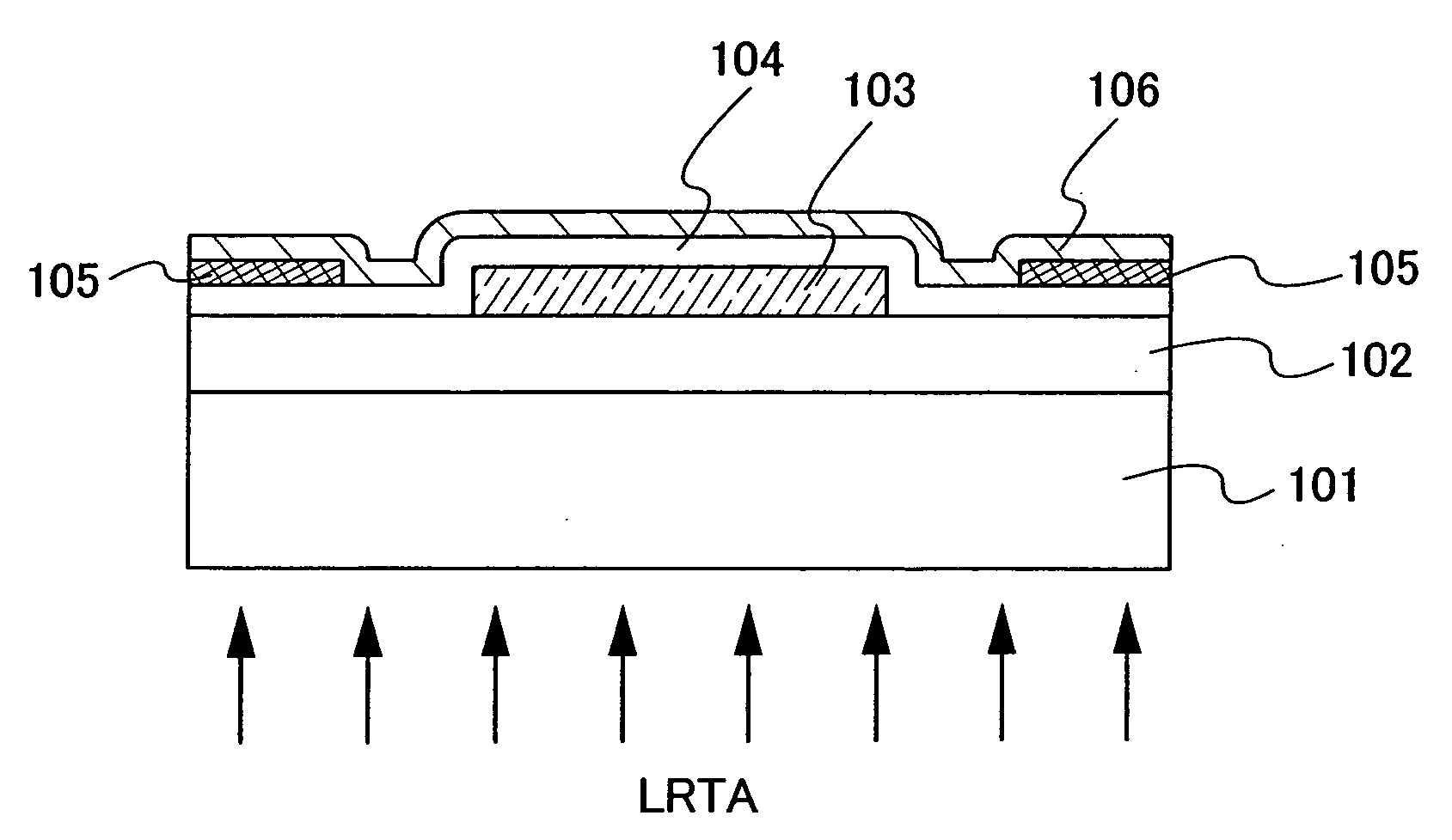
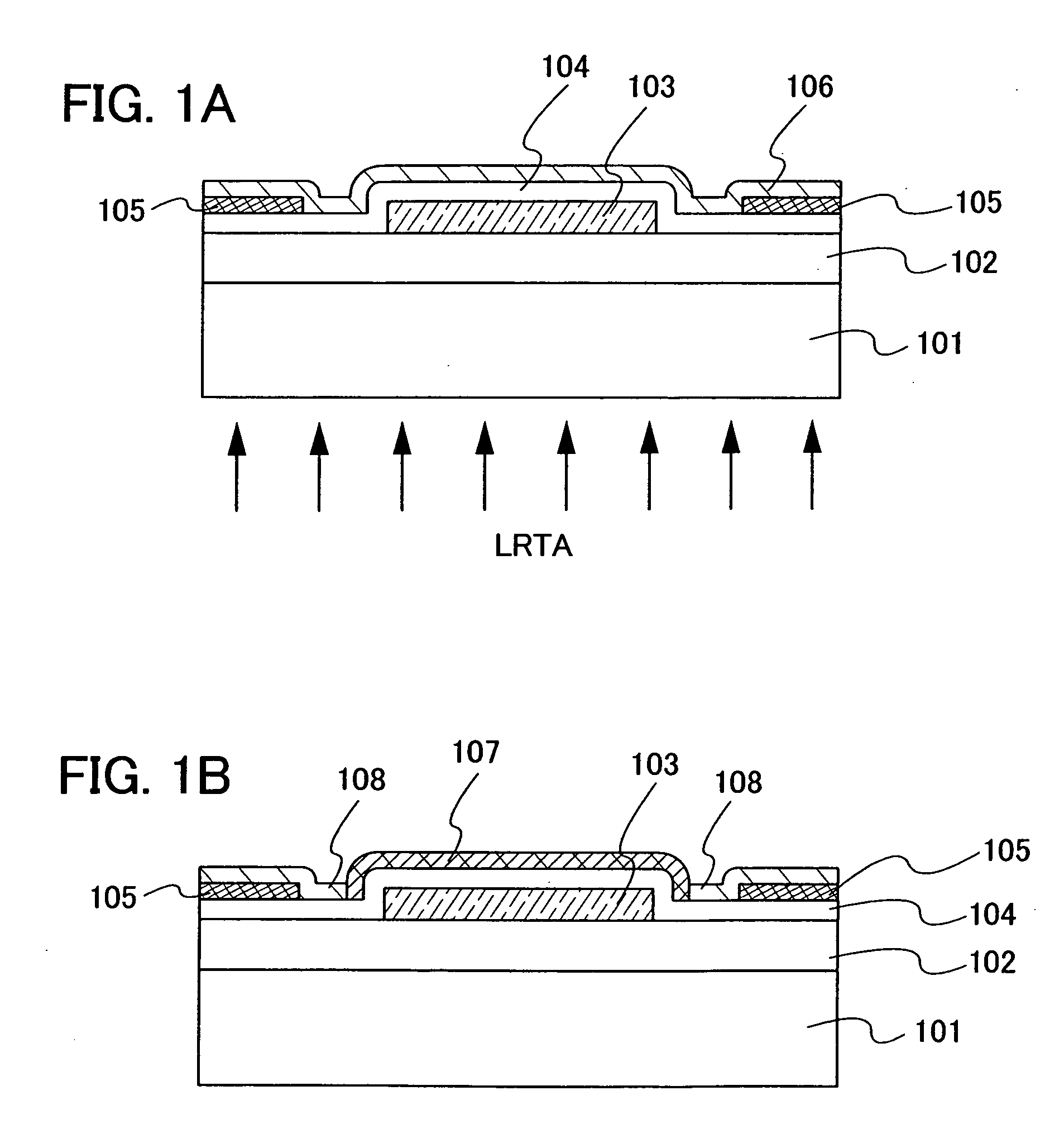
[0071] In this embodiment mode, a manufacturing step of a TFT using a channel forming as a region of an oxide semiconductor film in which crystallinity is improved by LRTA, is described with reference to FIGS. 1A and 1B.
[0072] First, a base film 102 is formed over a substrate 101. For the substrate 101, glass, or plastic (synthetic resin) such as polyethylene terephthalate (PET), polyethylene naphthalate (PEN), polyether sulfone (PES), acrylic, or polyimide can be used.
[0073] As the base film 102, a single layer of an insulating film such as a silicon oxide film, a silicon nitride film, a silicon oxynitride film (SiOxNy) (x>y), or a silicon nitride oxide film (SiNxOy) (x>y), or stacked layers thereof are used. The base film 102 may be formed by a sputtering method or a CVD method. Note that the base film 102 is not always required to be provided, but it is preferable to form in the present invention. By forming the base film 102, conduction of heat generated fro...
embodiment mode 2
(Embodiment Mode 2)
[0087] In this embodiment mode, a structure that is different from that in Embodiment Mode 1 is described with reference to FIGS. 3A to 3C. Note that steps of forming a base film 302, a gate electrode 303, and a gate insulating film 304 over a substrate 301 corresponds to the steps of forming the base film 102, the gate electrode 103, and the gate insulating film 104 over the substrate 101 of Embodiment Mode 1, respectively; therefore, refer to Embodiment Mode 1 for the steps.
[0088] A first oxide semiconductor film 305 is formed over the gate insulating film 304. For the oxide semiconductor film 305, zinc oxide (ZnO) in an amorphous state, a polycrystalline state, or a microcrystalline state in which both amorphous and polycrystalline states exist, added with one type or a plurality of types of impurity elements selected from Group 1 elements, Group 13 elements, Group 14 elements, Group 15 elements, and Group 17 elements can be used. Alternatively, zinc oxide (Zn...
embodiment mode 3
(Embodiment Mode 3)
[0096] An embodiment mode of the present invention is described with reference to FIGS. 4A to 5C. This embodiment mode is an example of a semiconductor device including a channel protective thin film transistor.
[0097] As a substrate 400, a glass substrate including barium borosilicate glass, alumino borosilicate glass, or the like; a silicon substrate; a plastic substrate having heat resistance; or a resin substrate is used. As the plastic substrate or the resin substrate, polyethylene terephthalate (PET), polyethylene naphthalate (PEN), polyether sulfone (PES), acrylic, polyimide, or the like can be used. Also, a surface of the substrate 400 may be polished by a CMP method so that the surface is planarized. Note that an insulating layer may be formed over the substrate 400. The insulating layer is formed to have a single layer structure or a stacked layer structure using at least one of an oxide material including silicon and a nitride material including silicon...
PUM
| Property | Measurement | Unit |
|---|---|---|
| temperature | aaaaa | aaaaa |
| wavelength region | aaaaa | aaaaa |
| temperature | aaaaa | aaaaa |
Abstract
Description
Claims
Application Information