

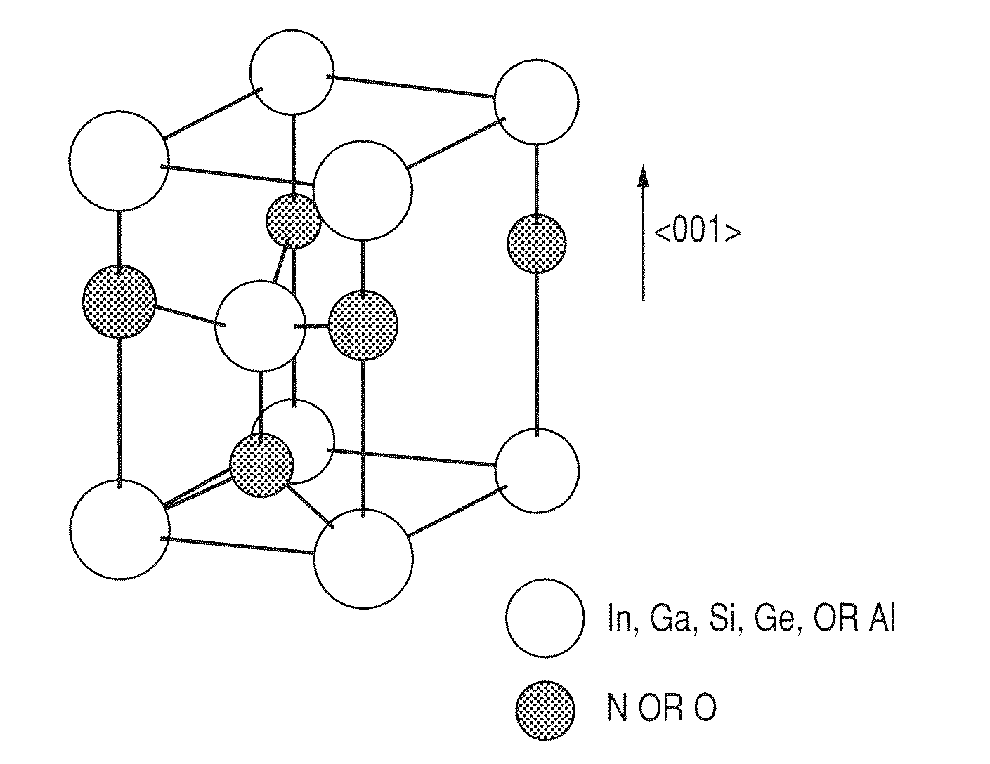
Substrate for growing wurtzite type crystal and method for manufacturing the same and semiconductor device
a technology of wurtzite type crystal and substrate, which is applied in the direction of crystal growth process, natural mineral layered products, polycrystalline material growth, etc., can solve the problem of not having a lattice constant largely different from that of the substrate layer, and it is difficult to obtain a crystal having a lattice constant largely different from that of the substrate layer, and achieves excellent crystallinity and low cost.
- Summary
- Abstract
- Description
- Claims
- Application Information
AI Technical Summary
Benefits of technology
Problems solved by technology
Method used
Image

Examples
example 1
ZnInON / GaN / Al2O3; Zn:In=37:20
[0082]In this Example, GaN was formed on a c-plane sapphire substrate by MOCVD, and then, a ZnInON film was formed by RF sputtering in an argon-nitrogen mixed atmosphere.
[0083]First, GaN was formed on the sapphire substrate by MOCVD. In this Example, annealing in a hydrogen atmosphere at 1150 degrees was performed as substrate pretreatment. Thus, high-quality GaN formed on the substrate is possible. It is known that in GaN growth, crystallinity in Ga polarity is higher than that in N polarity. This is because the GaN growth mode is in Ga polarity due to the pretreatment. The cause is not clear, but it is considered that the factor is that oxygen is reduced or etched by the pretreatment, so that the substrate surface is Al-richer than the stoichiometric ratio.
[0084]Then, the substrate temperature was lowered to 470 degrees, and trimethylgallium (TMG) as the Ga raw material, and ammonia as the N raw material were flowed to form a 20 nm GaN low-temperature ...
example 2
ZnInON / GaN / Al2O3; Zn:In=31:18
[0109]In this Example, GaN was formed on a c-plane sapphire substrate by MOCVD, and then, a ZnInON film was formed by RF sputtering in an argon-nitrogen mixed atmosphere.
[0110]First, GaN was formed on the sapphire substrate by MOCVD. In this Example, annealing in a hydrogen atmosphere at 1150 degrees was performed as substrate pretreatment. Thus, high-quality GaN formed on the substrate is possible. It is known that in GaN growth, crystallinity in Ga polarity is higher than that in N polarity. This is because the GaN growth mode is in Ga polarity due to the pretreatment. The cause is not clear, but it is considered that the factor is that oxygen is reduced or etched by the pretreatment, so that the substrate surface is Al-richer than the stoichiometric ratio. Then, the substrate temperature was lowered to 470 degrees, and trimethylgallium (TMG) as the Ga raw material, and ammonia as the N raw material were flowed to form a 20 nm GaN low-temperature buffe...
example 3
ZnInON / GaN / Al2O3; Zn / In Composition Dependence
[0130]In this Example, GaN was formed on a c-plane sapphire substrate by MOCVD, and then, a ZnInON film was formed by RF sputtering in an argon-nitrogen mixed atmosphere.
[0131]First, GaN was formed on the sapphire substrate by MOCVD. In this Example, annealing in a hydrogen atmosphere at 1150 degrees was performed as substrate pretreatment. Thus, high-quality GaN formed on the substrate is possible. It is known that in GaN growth, crystallinity in Ga polarity is higher than that in N polarity. This is because the GaN growth mode is in Ga polarity due to the pretreatment. The cause is not clear, but it is considered that the factor is that oxygen is reduced or etched by the pretreatment, so that the substrate surface is Al-richer than the stoichiometric ratio.
[0132]Then, the substrate temperature was lowered to 470 degrees, and trimethylgallium (TMG) as the Ga raw material, and ammonia as the N raw material were flowed to form a 20 nm GaN...
PUM
| Property | Measurement | Unit |
|---|---|---|
| lattice constant | aaaaa | aaaaa |
| optical band gap | aaaaa | aaaaa |
| optical band gap | aaaaa | aaaaa |
Abstract
Description
Claims
Application Information