Structure with transistor

a technology of structure and transistor, applied in the field of flexible transistor, can solve the problems of difficult to realize a flexible transistor, low mobility of organic semiconductor, and inability to use organic semiconductors in practical use, and achieve the effect of high mobility and on/off ratio

Active Publication Date: 2008-10-23
TOPPAN PRINTING CO LTD
View PDF5 Cites 3850 Cited by
  • Summary
  • Abstract
  • Description
  • Claims
  • Application Information

AI Technical Summary

Benefits of technology

[0016]One embodiment of the present invention is disclosed. In the present invention, oxygen and water vapor from a substrate are shielded by a gas barrier layer, and they do not go to an oxi

Problems solved by technology

Therefore, it was difficult to realize a flexible transistor with the use of an inexpensive plastic substrate.
However, mobility of organic semiconductor is extremely low.
Therefore, practical use of organic semiconductor has n

Method used


Image

  • Structure with transistor
  • Structure with transistor
  • Structure with transistor

Examples


examples

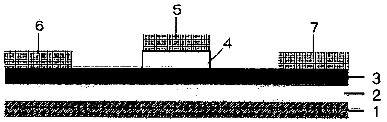
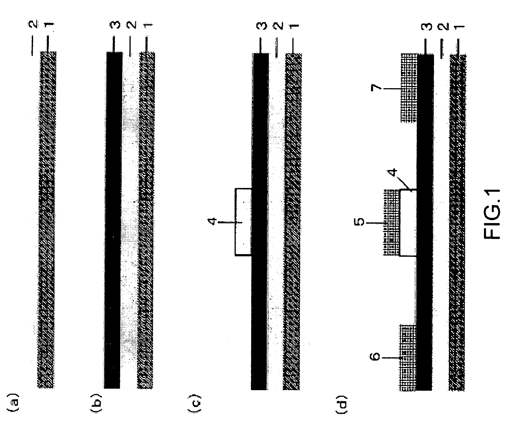
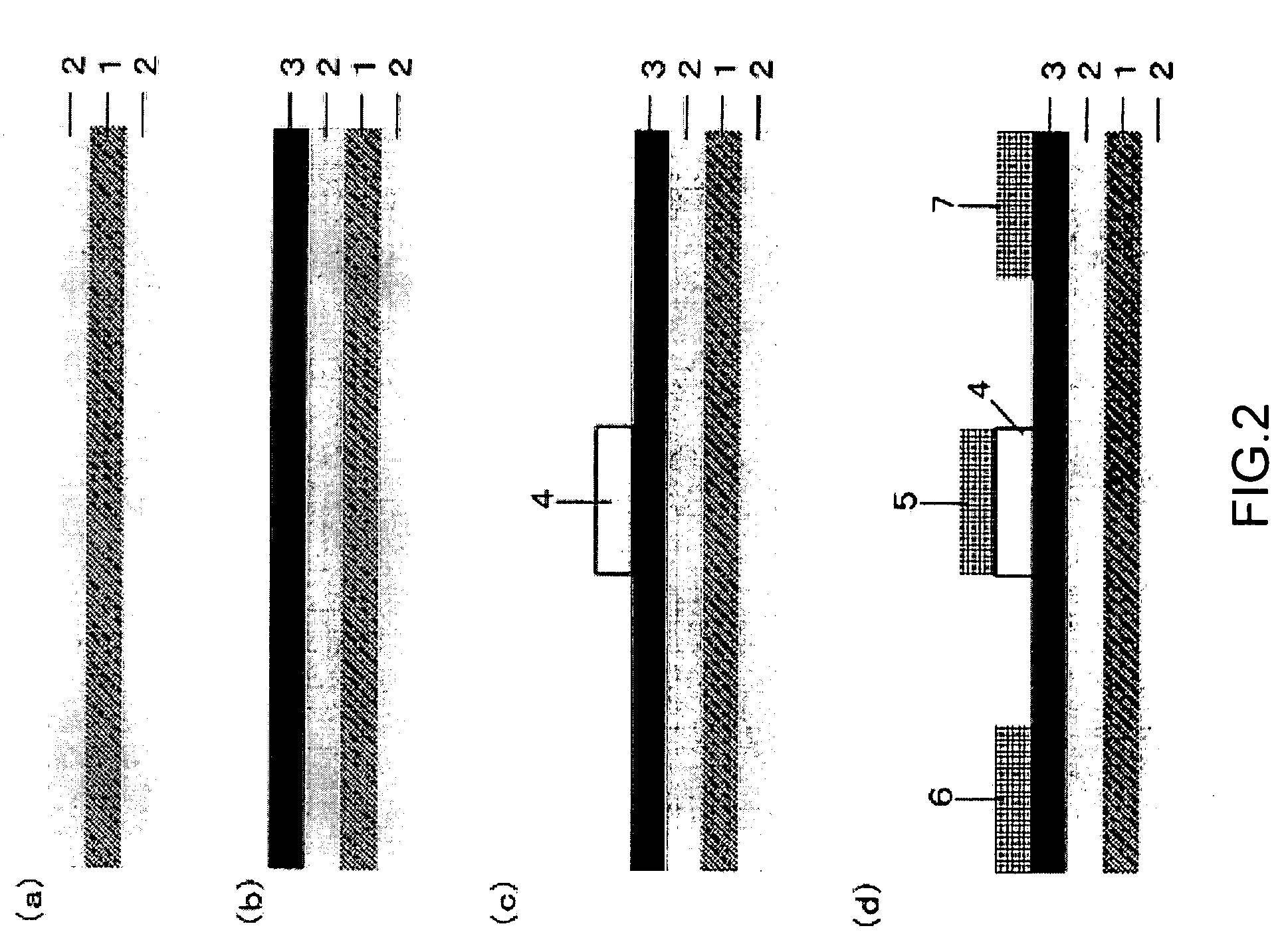
[0055]At first, aluminium oxide of different thickness was deposited on polyethylene terephthalate (PET) of 100 μm thickness by continuous roll-to-roll evaporation method using electron beam thermal process. Then, gas barrier property (water vapor transmission rate, oxygen transmission rate) was measured. In addition, to raise gas barrier property, aluminium oxide was deposited on both sides of PET film in Example 1, 2, 11, 12 and 13. (In addition, aluminium oxide was not deposited on PET film in Comparative Example.)

[0056]A semiconductor layer having film thickness of 40 nm was made on the PET with deposited aluminium oxide by RF magnetron sputtering technique [sputtering gas: Ar 19.4 SCCM, oxygen 0.6 SCCM (oxygen flow rate ratio 3%)] using InGaZnO4 as a sputter target.

[0057]A gate insulator having film thickness of 170 nm comprising Y2O3 was made on one part of this semiconductor layer by RF magnetron sputtering technique [sputtering gas: Ar 1 SCCM, oxygen 20 SCCM] using Y2O3 as a...


PUM


Abstract

A structure with a transistor is disclosed comprising a substrate, a gas barrier layer on the substrate, and a transistor on the gas barrier layer. The transistor can include an oxide semiconductor layer. The oxide semiconductor layers can comprise In—Ga—Zn—O. A display, such as a liquid crystal display, can have such a structure.

Description

BACKGROUND OF THE INVENTION[0001]1. Field of the Invention[0002]The present invention is related to a flexible transistor having an oxide semiconductor layer.[0003]A transistor of the present invention can be used for devices such as a liquid crystal display, an organic light emitting display, a micro capsule type electrophoresis-type display, a photo-write type cholesteric liquid crystal type display, a TwistingBall type display, a toner type display, a movable film type display and an RFID (RadioFrequencyIdentification) sensor.[0004]2. Description of the Related Art[0005]Generally the transistor which used an amorphous silicon semi-conductor or a polysilicon semi-conductor as a driving transistor of electron device has been used. However, film formation temperature equal to or more than 200 degrees Celsius is required for manufacture of an amorphous silicon semi-conductor and polysilicon semi-conductor of high quality. Therefore, it was difficult to realize a flexible transistor w...

Claims


Application Information

Patent Timeline
IPC IPC(8): H01L21/16
CPCH01L29/78603H01L29/7869
Inventor ITO, MANABUKON, MASATOISHIZAKI, MANORUSEKINE, NORIMASA
Owner TOPPAN PRINTING CO LTD
Why Eureka
Try Eureka