Thin film transistor having oxide semiconductor layer and manufacturing method thereof

a technology of thin film transistor and semiconductor layer, which is applied in the direction of semiconductor devices, instruments, electrical equipment, etc., can solve the problems of lowering process accuracy, and achieve the effects of low etching resistance, easy melting, and large side etching

Active Publication Date: 2006-12-21
SAMSUNG DISPLAY CO LTD
View PDF14 Cites 3803 Cited by
  • Summary
  • Abstract
  • Description
  • Claims
  • Application Information

AI Technical Summary

Benefits of technology

[0006] However, according to the above-described manufacturing method, it has been turned out that since zinc oxide easily melts in both acid and alkali and has a greatly low etching resistance, the semiconductor thin film and ohmic contact layer made of zinc oxide formed in the device area suffer a relatively large side etching in the manufacturing steps to follow, lowering the process accuracy.

Problems solved by technology

However, according to the above-described manufacturing method, it has been turned out that since zinc oxide easily melts in both acid and alkali and has a greatly low etching resistance, the semiconductor thin film and ohmic contact layer made of zinc oxide formed in the device area suffer a relatively large side etching in the manufacturing steps to follow, lowering the process accuracy.

Method used


Image

  • Thin film transistor having oxide semiconductor layer and manufacturing method thereof
  • Thin film transistor having oxide semiconductor layer and manufacturing method thereof
  • Thin film transistor having oxide semiconductor layer and manufacturing method thereof

Examples


first embodiment

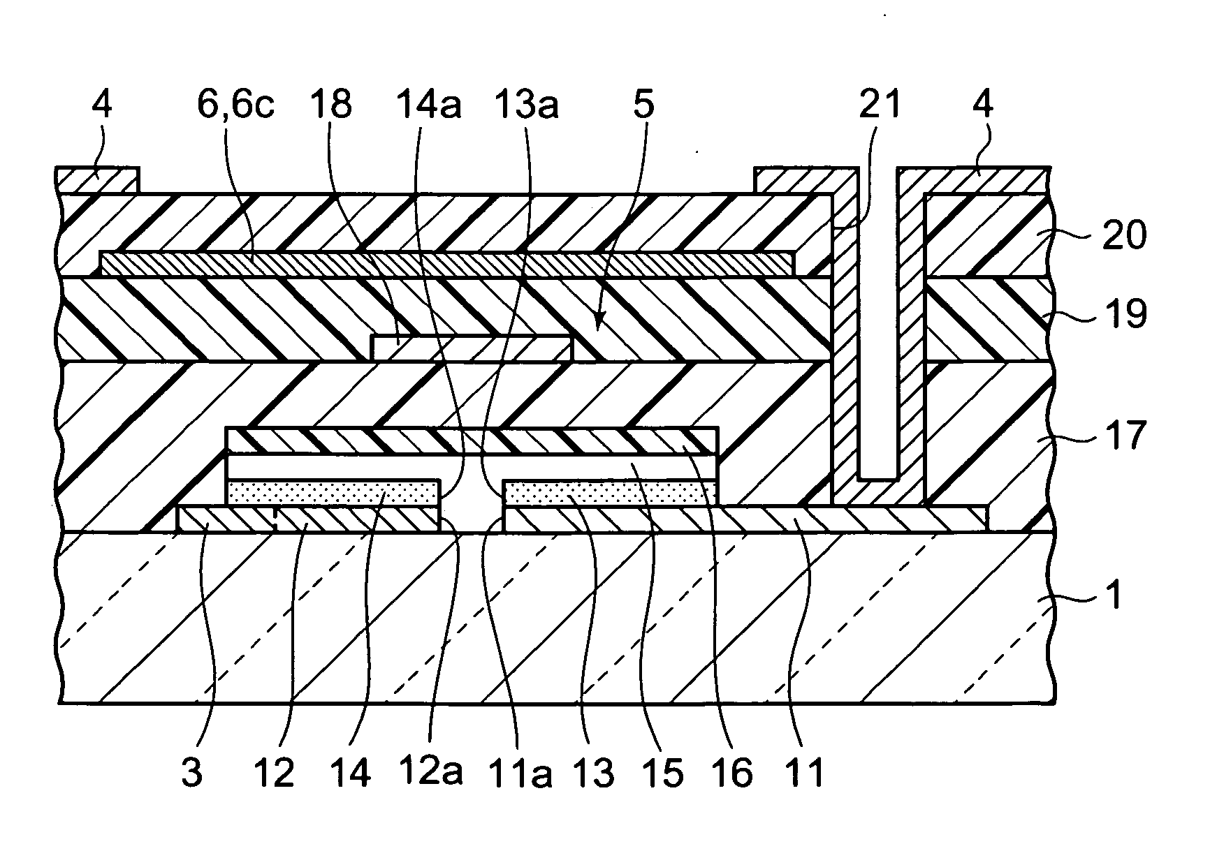
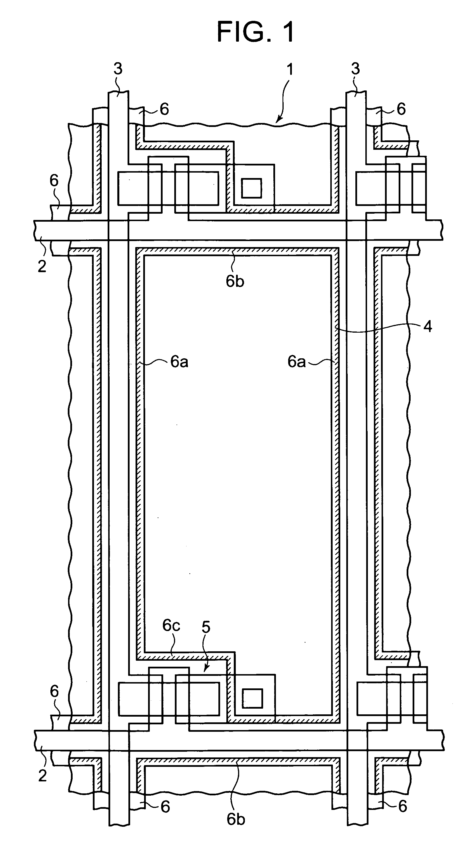
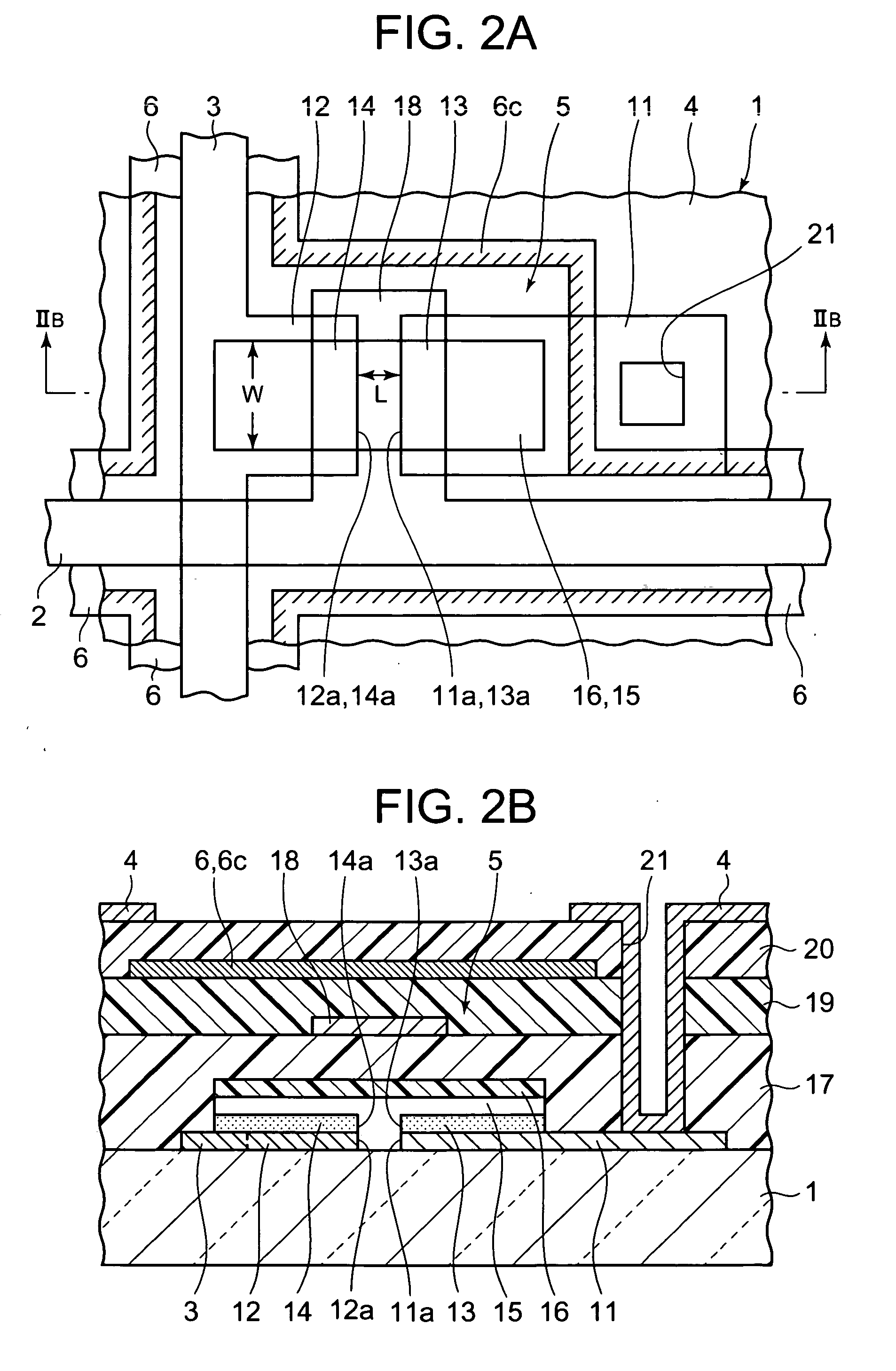
[0027]FIG. 1 shows a see-through plan view of the principal part of a liquid crystal display device comprising a thin film transistor as the first embodiment of the present invention. FIG. 2A shows an expanded see-through plan view of a part of FIG. 1, and FIG. 2B shows a cross sectional view as sectioned along a line IIB-IIB of FIG. 2A. The liquid crystal display device has a grass substrate 1.

[0028] Explanation will first be given with reference to FIG. 1. Scanning lines 2 and data lines 3 are formed in a matrix form on the upper surface of the grass substrate 1. A pixel electrode 4 is formed in the region surrounded by the scanning lines 2 and data lines 3, so as to be connected to a scanning line 2 and a data line 3 via a thin film transistor 5. A latticed auxiliary capacitor electrode 6 is formed in parallel with the scanning lines 2 and data lines 3. Note that hatching of angled short solid lines is used at the edges of the pixel electrode 4, throughout the drawings including...

second embodiment

[0057]FIG. 10A shows a see-through plan view of a principal part of a liquid crystal display device comprising a thin film transistor, as the second embodiment of the present invention. FIG. 10B shows a cross sectional view as sectioned along an XB-XB line of FIG. 10A. The difference between the present liquid crystal display device and the liquid crystal display device shown in FIG. 2A and FIG. 2B is that one ohmic contact layer 13 is formed at a predetermined position on the upper surface of the source electrode 11 at a side closer to the drain electrode 12 and on the neighboring upper surface of the grass substrate 1, and the other ohmic contact layer 14 is formed at a predetermined position on the upper surface of the drain electrode 12 including a part of the data line 3 at a side closer to the source electrode 11 and on the neighboring upper surface of the grass substrate 1. That is, the ohmic contact layers 13 and 14 are formed on the upper surfaces of the source electrode 11...

third embodiment

[0069]FIG. 16A shows a see-through plan view of a principal part of a liquid crystal display device comprising a thin film transistor, as the third embodiment of the present invention. FIG. 16B shows a cross-sectional view as sectioned along a ling XVIB-XVIB of FIG. 16A. The difference between the present liquid crystal display device and the liquid crystal display device shown in FIG. 2A and FIG. 2B is that no upper insulating film 19 is formed but the gate electrode 18, the scanning line 2 connected to the gate electrode 18, and the auxiliary capacitor electrode 6, which are made of a light blocking metal such as aluminum, chromium, etc., are formed at respective predetermined positions on the upper surface of the insulating film 17, and the gate electrode 18, the scanning line 2, and the auxiliary capacitor electrode 6 are covered with the overcoat film (insulating film) 20a.

[0070] In this case, the auxiliary capacitor electrode 6 comprises a first auxiliary capacitor electrode ...


PUM


Abstract

A thin film transistor has a semiconductor thin film including zinc oxide, a protection film formed on entirely the upper surface of the semiconductor thin film, a gate insulating film formed on the protection film, a gate electrode formed on the gate insulating film above the semiconductor thin film, and a source electrode and drain electrode formed under the semiconductor thin film so as to be electrically connected to the semiconductor thin film.

Description

BACKGROUND OF THE INVENTION [0001] 1. Field of the Invention [0002] The present invention relates to a thin film transistor, and particularly relates to a thin film transistor suitable for a case where its semiconductor layer is an oxide semiconductor layer. [0003] 2. Description of the Related Art [0004] As described in Unexamined Japanese Patent Application KOKAI Publication No. H5-67786, an inversely staggered structure is generally adopted for a thin film transistor used as a switching element of an active matrix liquid crystal display device. A thin film transistor of this structure is constructed such that a gate electrode is formed on an insulating substrate, a gate insulating film is formed on the upper surface of the gate electrode and insulating substrate, a semiconductor thin film made of intrinsic amorphous silicon is formed on the upper surface of the gate insulating film that is on the gate electrode, a channel protection film is formed on the center portion of the upp...

Claims


Application Information

Patent Timeline
Patent Type & Authority Applications(United States)
IPC IPC(8): H01L29/76H01L29/12H01L21/8234
CPCH01L29/7869G02F1/1368H01L27/1225H01L29/66969H01L29/458
Inventor ISHII, HIROMITSU
Owner SAMSUNG DISPLAY CO LTD
Why Eureka
Try Eureka