
Method of producing a reflective mask

a reflective mask and mask body technology, applied in the field of reflective mask production, can solve the problems of reducing the reflectance, insufficient anti-oxidation effect, disadvantage of ru film, etc., and achieve the effect of excellent chemical resistance and excellent resistance to an environmen

Inactive Publication Date: 2010-04-08
HOYA CORP
View PDF0 Cites 8 Cited by
  • Summary
  • Abstract
  • Description
  • Claims
  • Application Information

AI Technical Summary

Benefits of technology

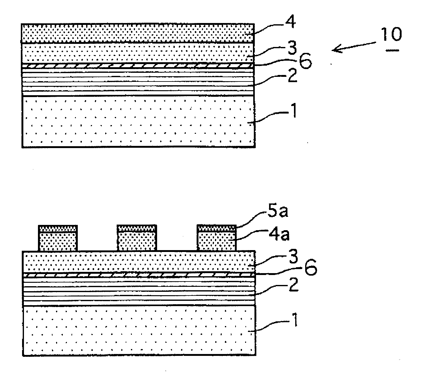
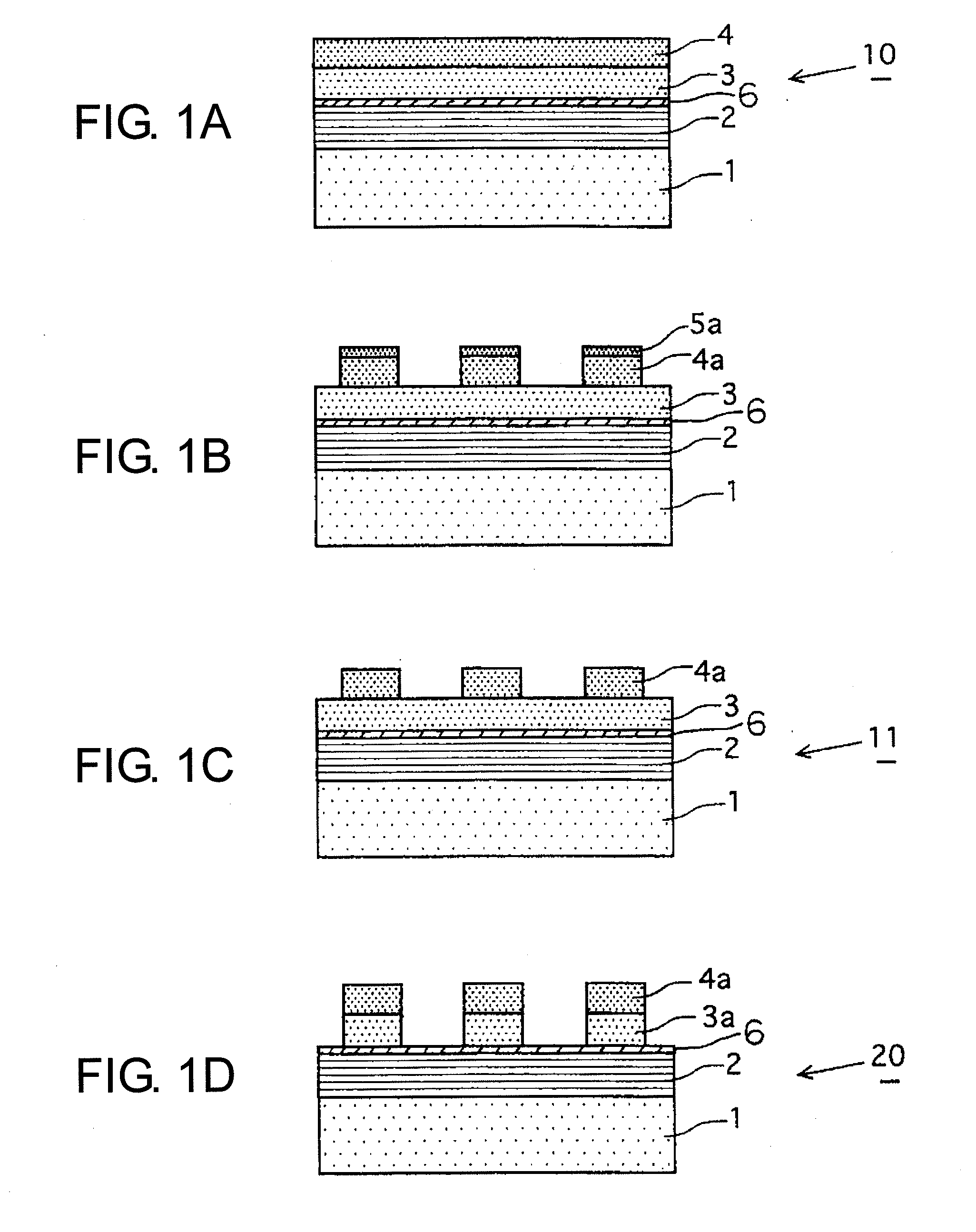
[0010]For example, in case where a Ta-based material is used as the absorber film, a Cr-based buffer film may be formed in order to prevent an etching damage of the multilayer reflective film during pattern formation. After the absorber film is patterned, the Cr-based buffer film is patterned according to the absorber pattern. Generally, the Cr-based buffer film is patterned by dry etching performed by the use of an oxygen-added chlorine-based gas. The above-mentioned Ru protective film is low in etching resistance particularly against an oxygen-added chlorine-based gas containing 70% or more oxygen. This results in occurrence of damage in the multilayer reflective film to cause decrease in reflectance.
[0035]According to this invention, it is possible to provide a method of producing a reflective mask having a protective film which is formed on a multilayer reflective film and which is excellent in resistance against an environment during pattern formation of a buffer film formed on the multilayer reflective film and excellent in chemical resistance during cleaning or the like.

Problems solved by technology

In this case, if the Si film is thin, a sufficient anti-oxidation effect is not achieved.
However, since the Si film slightly absorbs the EUV light, the large thickness of the Si film disadvantageously results in decrease of the reflectance.
However, the Ru film is disadvantageous in the following respects.
The above-mentioned Ru protective film is low in etching resistance particularly against an oxygen-added chlorine-based gas containing 70% or more oxygen.
This results in occurrence of damage in the multilayer reflective film to cause decrease in reflectance.

Method used


Image

  • Method of producing a reflective mask
  • Method of producing a reflective mask
  • Method of producing a reflective mask

Examples


example 1

[0084]A SiO2—TiO2 glass substrate (6-inch square, 6.3 mm thick) was used as a substrate. The glass substrate had a coefficient of thermal expansion of 0.2×10⁻⁷ / ° C. and a Young's modulus of 67 GPa. The glass substrate was polished by mechanical polishing to have a smooth surface of 0.2 nmRms or less and a flatness of 100 nm or less.

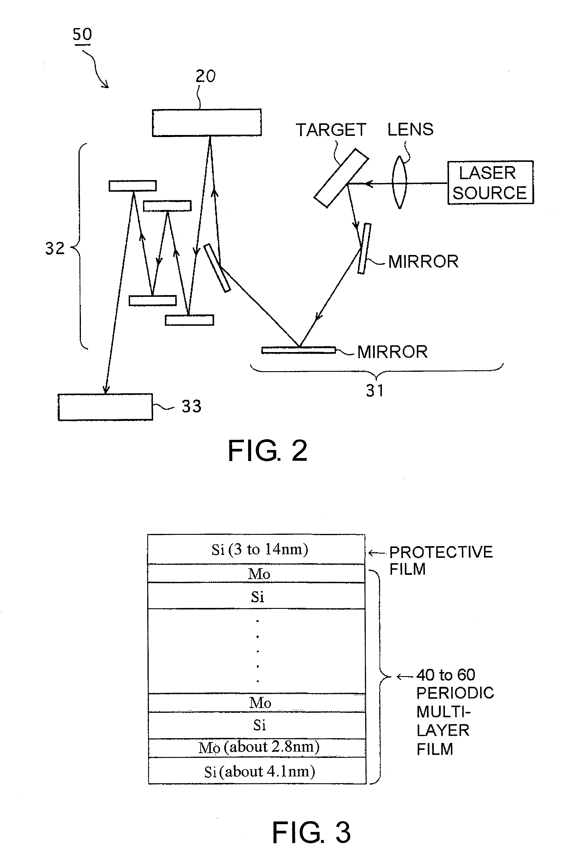
[0085]As a multilayer reflective film formed on the substrate, a periodic Mo / Si multilayer reflective film was used so as to be suitable for an exposure wavelength band between 13 and 14 nm. Specifically, the multilayer reflective film was formed by alternately laminating Mo and Si films on the substrate by ion beam sputtering using a Mo target and a Si target. Herein, a combination of the Si film having a thickness of 4.2 nm and the Mo film having a thickness of 2.8 nm is defined as a single period. After these films were laminated in 40 periods, deposition of the Si film to a thickness of 4.2 nm was performed at an end of deposition of the multilayer re...


PUM


Abstract

A method of producing a reflective mask is carried out by the use of a reflective mask blank which has a substrate, a multilayer reflective film formed on the substrate to reflect exposure light, a protective film formed on the multilayer reflective film, a buffer film formed on the protective film, and an absorber film formed on the buffer film to absorb the exposure light. The protective film is made of a ruthenium compound containing Ru and Nb. The method includes a step of patterning the buffer film by dry etching performed by the use of an etching gas containing oxygen.

Description

[0001]This application is based upon and claims the benefit of priority from Japanese Patent Application No. 2008-259138, filed on Oct. 4, 2008, and Japanese Patent Application No. 2009-214524, filed on Sep. 16, 2009, the disclosures of which are incorporated herein in their entirety by reference.BACKGROUND OF THE INVENTION[0002]This invention relates to a method of producing a reflective mask for exposure which is for use in manufacture of a semiconductor device and the like.[0003]In recent years, the advance of miniaturization of semiconductor devices awakens expectations of using EUV lithography as an exposure technique using extreme ultra violet (hereinafter abbreviated to EUV) light in the semiconductor industry. Herein, the EUV light represents light in a wavelength band of a soft X-ray region or a vacuum ultraviolet region and, specifically, light having a wavelength of approximately 0.2 to 100 nm. As a mask for use in the EUV lithography, a reflective mask for exposure is pr...

Claims


Application Information

Patent Timeline
IPC IPC(8): B44C1/22G03F1/22G03F1/24H01L21/027
CPCG03F1/24G03F1/48G03F7/091H01L21/0332
Inventor HOSOYA, MORIO
Owner HOYA CORP
Learn More