

MEMS device, electronic apparatus, and manufacturing method of MEMS device
a manufacturing method and technology of a mems device, applied in the direction of microstructural devices, microstructured devices, microstructured technology, etc., can solve the problems of etching for forming the cavity, and reducing reliability of the device, so as to achieve a further simplified management and high reliability
- Summary
- Abstract
- Description
- Claims
- Application Information
AI Technical Summary
Benefits of technology
Problems solved by technology
Method used
Image

Examples
embodiment 1
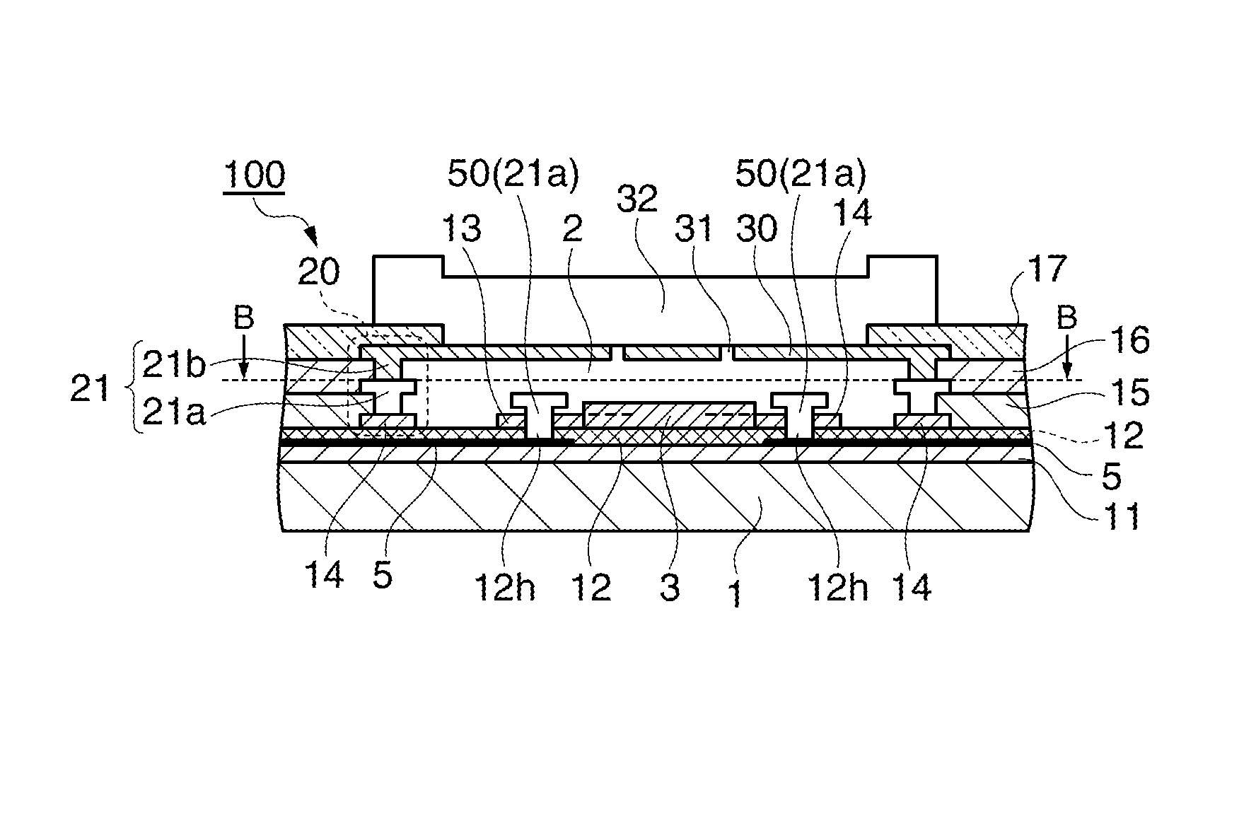
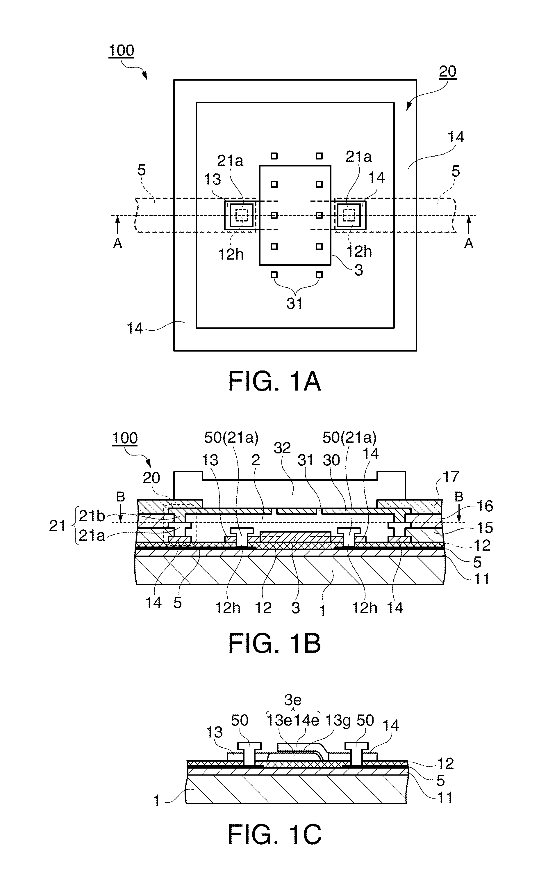
[0037]FIG. 1A is a plan view illustrating a MEMS device 100 according to Embodiment 1, FIG. 1B is a cross-sectional view taken along the line A-A of FIG. 1A, and FIG. 1C is a cross-sectional view illustrating an example of a MEMS structure.
[0038]FIG. 1A is a plan view taken along the line B-B of FIG. 1B. In addition, in FIG. 1A, openings 31 are also shown for better understanding.
[0039]A MEMS device 100 is a MEMS device having a MEMS structure (an electro-mechanical system structure having a mechanically movable structure) disposed in a cavity portion which is formed by etching a sacrificial layer laminated on a main surface of a wafer substrate.
[0040]The MEMS device 100 includes a wafer substrate 1, a cavity portion 2, a MEMS structure 3, a lower-layer wire portion 5, a first oxide film 11 which is a first insulating layer, a nitride film 12 which is a second insulating layer, a first conductive layer 13, a second conductive layer 14, a second oxide film 15, a third oxide film 16, ...
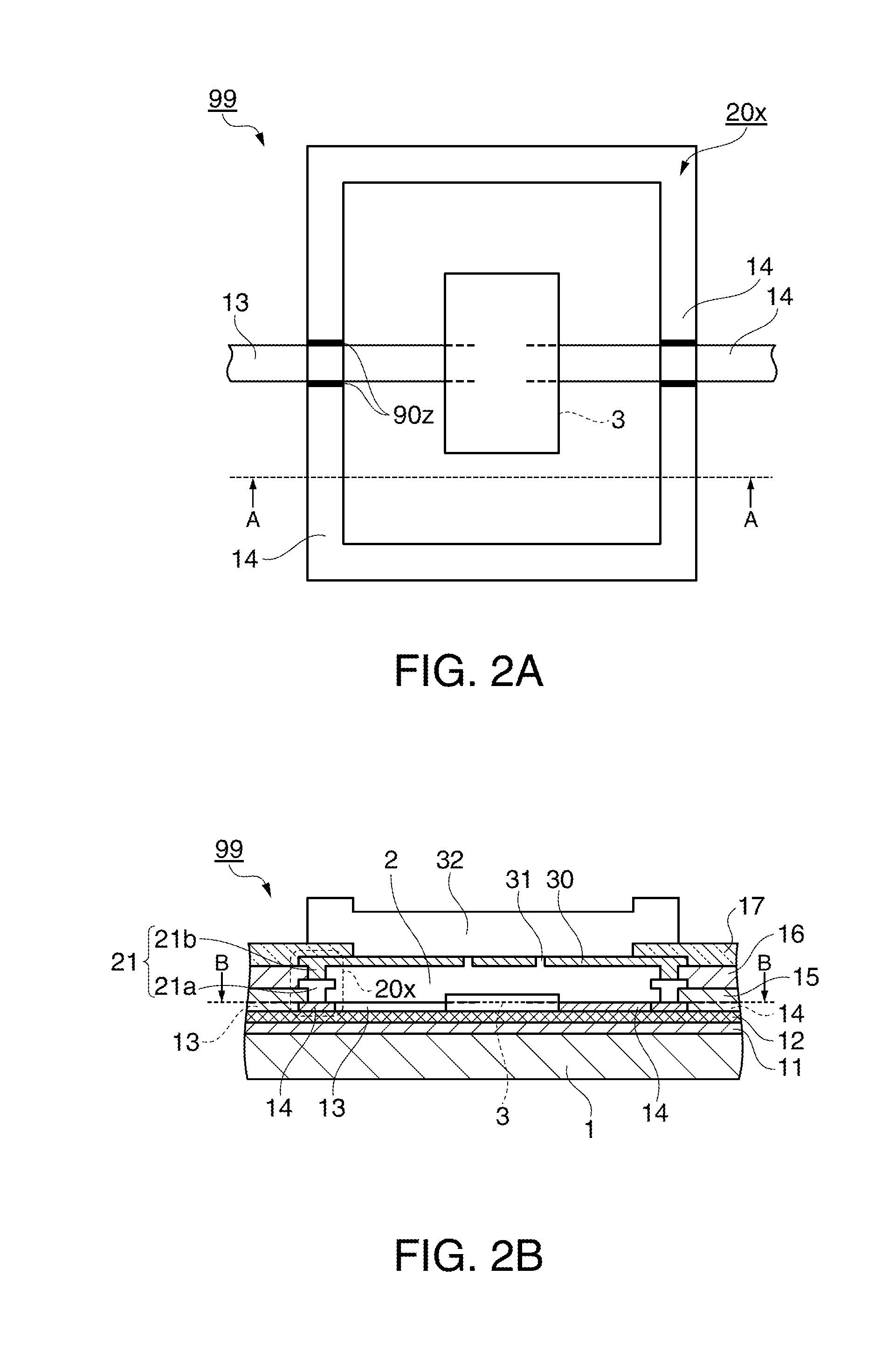
modification examples
[0106]A method of connection to the first conductive layer 13 or the second conductive layer 14 at the upper part of the electrical connection portion 50 is not limited to the configuration of Embodiment 1, and may have the following configurations.
[0107]FIGS. 6A and 6B are cross-sectional views illustrating variations of a method of connection of the electrical connection portion 50 to a first conductive layer 13 or a second conductive layer 14 at the upper part of the electrical connection portion 50 as modification examples. In either case, there is a feature in which the area of the electrical connection portion 50 is larger than the area of the through hole 12h in plan view of the wafer substrate 1.
[0108]In the example shown in FIG. 6A, an upper part of an electrical connection portion 50a is formed so as to expand on the first conductive layer 13 or the second conductive layer through patterning using photolithography, thereby increasing the number of contact parts or the cont...
PUM
| Property | Measurement | Unit |
|---|---|---|
| electrical | aaaaa | aaaaa |
| area | aaaaa | aaaaa |
| capacitance | aaaaa | aaaaa |
Abstract
Description
Claims
Application Information