Dry etching method for oxide semiconductor film

a technology of oxide semiconductor film and etching method, which is applied in the direction of semiconductor devices, decorative arts, photovoltaic energy generation, etc., can solve the problems of high temperature melted and deformed photoresist, low production yield, and liable to break the wiring provided through the patterned edge, etc., to achieve high etching rate, high processing accuracy, and high processing accuracy

Inactive Publication Date: 2007-12-13
CANON KK
View PDF4 Cites 3762 Cited by
  • Summary
  • Abstract
  • Description
  • Claims
  • Application Information

AI Technical Summary

Benefits of technology

[0018]In order to solve the above-mentioned problems, it is an object of the present invention to provide a method of processing a film made of In—Ga—Zn—O with high processing accuracy. That is, it...

Problems solved by technology

However, the lift-off method has a problem in that a photoresist is melted and deformed at high temperature.
Further, the lift-off method has another problem in that, in removing a photoresist, a patterned edge of a film to be vapor-deposited rides up, with the result that wirings provided through the patterned edge are liable to be broken and the production yield is low.
In this case, there arises a problem in that it is difficult to remove a nonvolatile material, which is deposited on a surface of the resist after the etching, even by cleaning with supersonic waves.
In principle, in the wet etching method, etching advances isotropically, which raises a problem in that a phenomenon such as undercut of a lower portion of a mask, corrosion of a pattern due to adhesion failure between a mask and a coated film, or penetration of an etchant occurs.
Further, there arises another problem in that etching residues float and remain on a device.
Accordingly, replacement of the etchant is required at high frequency, which may lead to a large consumption of the etchant.
However, the above-mentioned cited references do not disclose a specific dry etching for In—Ga—Zn—O, or include embodiments thereof.
The dry etching of the film made of In—Ga—Zn—O using CF4 is disadvantageous for mass production in that the e...

Method used


Image

  • Dry etching method for oxide semiconductor film
  • Dry etching method for oxide semiconductor film
  • Dry etching method for oxide semiconductor film

Examples


example 1

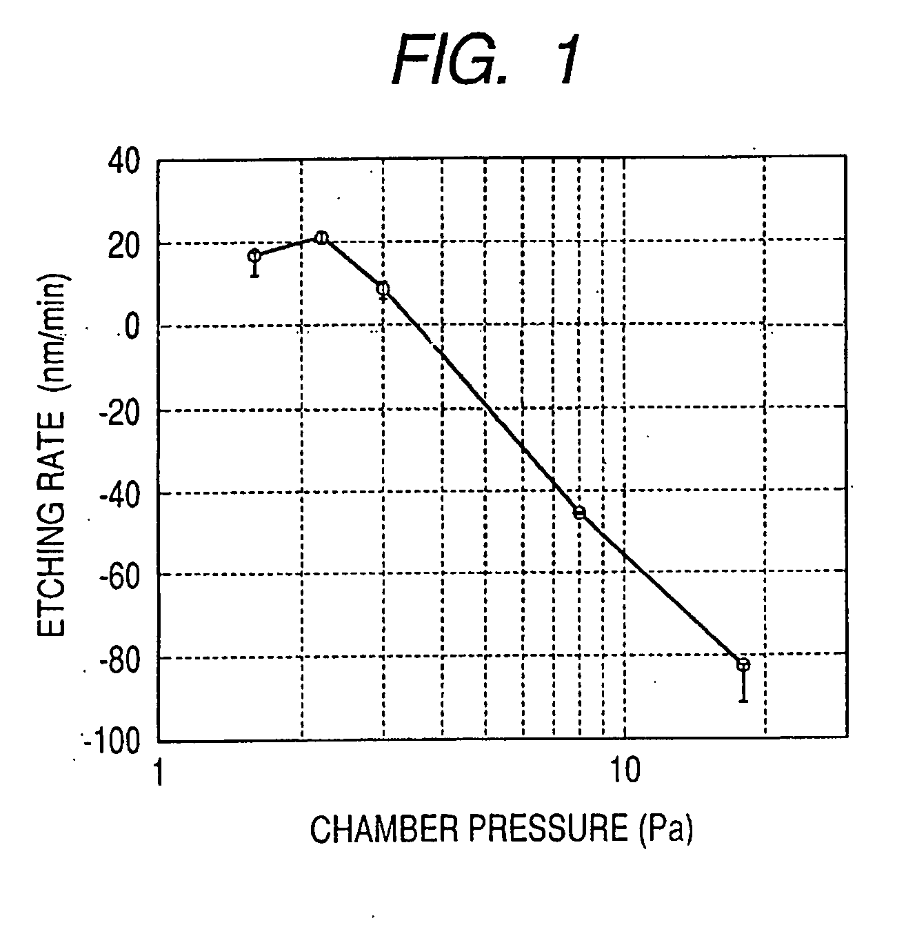
[0053]In Example 1, pressure dependency of an etching effect was observed. The observation of the pressure dependency was performed under such conditions that temperature was set to a room temperature, a pure CH4 flow rate was 38.7 sccm, and an RF power was 100 W (2.2 W / cm2). Results of the observation are illustrated in FIG. 1. An axis of abscissa indicates a chamber pressure, and an axis of ordinate indicates an etching rate. In FIG. 1, each negative value of the etching rate indicates a formation rate of a deposit. As a result, it was found that the dry etching can be excellently performed without forming a nonvolatile deposit in a case where the pressure was 3.5 Pa or lower. Note that, in the etching apparatus of this example, it was found that plasma was hardly excited in a case were the pressure was 0.6 Pa or lower. The lower the reactive pressure is set, the more the generation of the deposit can be suppressed. Accordingly, as long as the plasma can be excited at lower pressu...

example 2

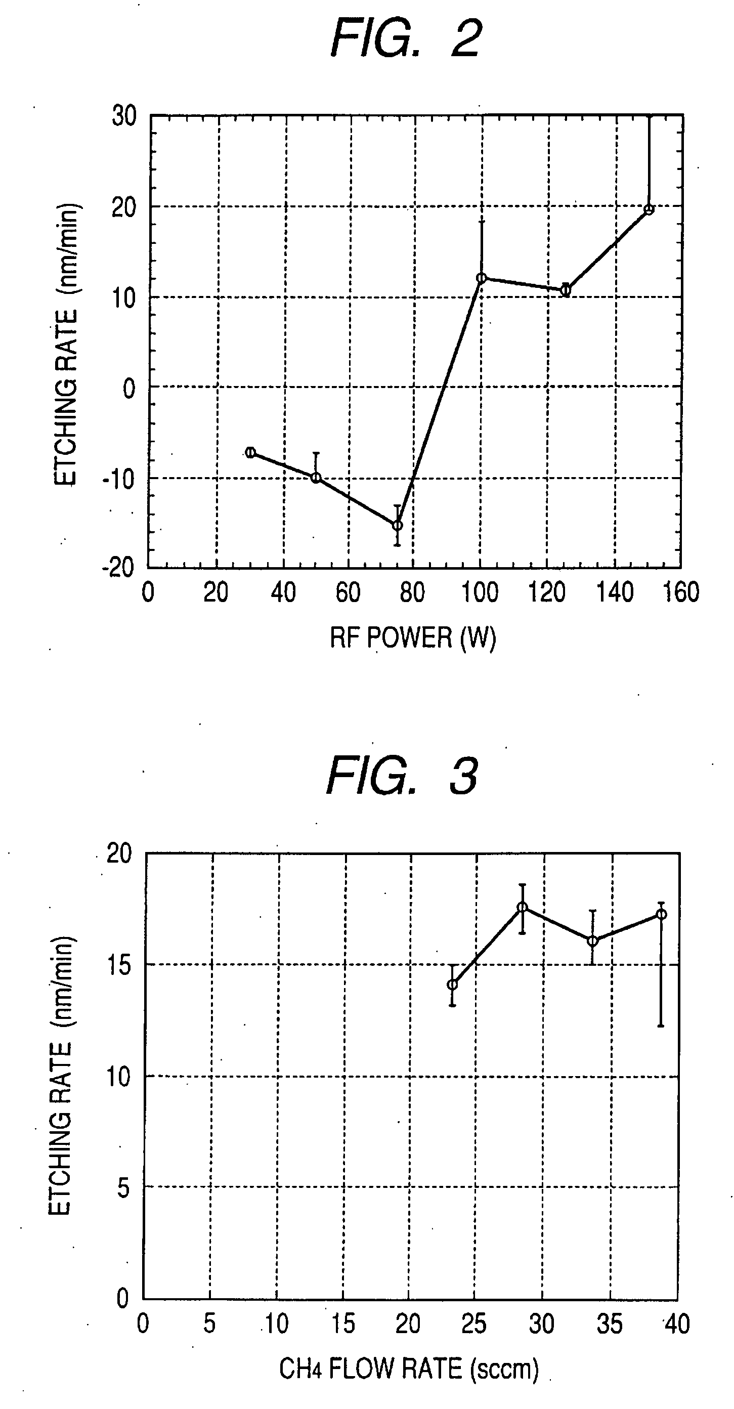
[0055]In Example 2, a relationship between an etching effect and an RF power was observed. The observation was performed under such conditions that temperature was set to a room temperature, a pure CH4 flow rate was 38.7 sccm, and a chamber pressure was 2.6 Pa. Results of the observation are illustrated in FIG. 2. An axis of abscissa indicates an RF power, and an axis of ordinate indicates an etching rate. In FIG. 2, each negative value of the etching rate indicates a formation rate of a deposit. As apparent from FIG. 2, it was found that the dry etching can be excellently performed without forming a nonvolatile deposit in a case where the RF power was 90 W or more. In a case were the RF power is 90 W or lower, the nonvolatile deposit is formed. It is assumed that, this is because, ions in the plasma have high kinetic energy when the RF power is high, and if a deposit may be formed, the deposit is to be etched again. In the etching apparatus of this example, an applied electrode has...

example 3

[0057]In Example 3, a relationship between an etching effect and a pure CH4 flow rate was observed. The observation was performed under such conditions that temperature was set to a room temperature, an RF power was 100 W (2.2 W / cm2), and a chamber pressure was 1.6 Pa. Results of the observation are illustrated in FIG. 3. An axis of abscissa indicates a CH4 flow rate, and an axis of ordinate indicates an etching rate. As apparent from FIG. 3, in a case where the CH4 flow rate is 23 sccm or lower, the plasma is hardly excited, so it is difficult to obtain data thereof. In a case were the CH4 flow rate is 23 sccm or more, it is found that the dry etching is excellently performed without forming the nonvolatile deposit. As illustrate in FIG. 3, it is assumed that, when the CH4 flow rate is 28 sccm or more, the CH4 flow rate is in a range of a surface reaction controlled rate, and when the CH4 flow rate is 28 sccm or lower, the CH4 flow rate is in a range of a supply controlled rate. In...


PUM

PropertyMeasurementUnit
Temperatureaaaaaaaaaa
Pressureaaaaaaaaaa

Abstract

Provided is a dry etching method for an oxide semiconductor film made of In—Ga—Zn—O, in which an etching gas containing a hydrocarbon is used in a dry etching process for the oxide semiconductor film made of In—Ga—Zn—O formed on a substrate.

Description

BACKGROUND OF THE INVENTION[0001]1. Field of the Invention[0002]The present invention relates to a dry etching method for an oxide containing In, Ga, and Zn (hereinafter, referred to as “In—Ga—Zn—O”), and more particularly, to a dry etching method for an oxide semiconductor In—Ga—Zn—O in manufacturing microelectronic components such as a semiconductor element, a semiconductor integrated circuit, ° and an electrode.[0003]2. Description of the Related Art[0004]As described in Japanese Patent Application Laid-Open No. 2004-103957, in recent years, research and development regarding a semiconductor film made of In—Ga—Zn—O and growth conditions for the semiconductor film have been conducted.[0005]K. Nomura et. al, Nature, vol. 432, 25 Nov. 2004, p. 488-492 and E. M. C. Fortunato et. al, Advanced Materials, 2005, 17, No. 5, p. 590-594 disclose that patterning of a produced film made of In—Ga—Zn—O or a film made of Ga—Zn—O has been performed by a lift-off method.[0006]Regarding the dry etc...

Claims


Application Information

Patent Timeline
IPC IPC(8): H01L21/465
CPCH01L21/465H01L29/7869H01L29/66969Y02E10/50H01L31/1884
Inventor CHANG, CHIENLIU
Owner CANON KK
Why Eureka
Try Eureka