Etching solution for multilayer thin film having copper layer and molybdenum layer contained therein

a multi-layer thin film and etching solution technology, which is applied in the direction of surface treatment compositions, semiconductor/solid-state device details, chemistry apparatus and processes, etc., can solve the problems of copper diffusion into the silicon semiconductor underlayer, the adhesiveness between the substrate such as glass or the like and copper is not sufficient, and the difficulty of uniform panel display, etc., to achieve good etching effect and low etching residue and unevenness, the effect of long bath li

Inactive Publication Date: 2012-12-20
MITSUBISHI GAS CHEM CO INC
View PDF13 Cites 11 Cited by
  • Summary
  • Abstract
  • Description
  • Claims
  • Application Information

AI Technical Summary

Benefits of technology

[0013]According to the present invention, there are provided an etching solution which secures, in an etching process for a multilayer thin film containing a copper layer and a molybdenum layer, high processing accuracy, little etching residue and unevenness and a long bath life, and realizes a good wiring profile after etching therewith, and which therefore can meet the requirement of size enlargement and resolution enhancement of displays, and an etching method using it for a multilayer thin film containing a copper layer and a molybdenum layer. According to the etching method, a wiring material that contains a multilayer thin film containing a copper layer and a molybdenum layer can be etched all at a time, and therefore, after etching therewith, a good wiring profile can be realized at high producibility.
[0014]The etching solution of the present invention is used for etching of a multilayer thin film having a copper layer and a molybdenum layer contained therein, and it comprises (A) hydrogen peroxide, (B) a fluorine atom-free inorganic acid, (C) an organic acid, (D) an amine compound having a carbon number of from 2 to 10 and having an amino group and a hydroxyl group in a total group number of 2 or more, (E) an azole, and (F) a hydrogen peroxide stabilizer, and has a pH of from 2.5 to 5.
[0015]Hydrogen peroxide which is used in the etching solution of the present invention has a function to oxidize a copper wiring as an oxidizing agent and also has a function to oxidize and dissolve molybdenum. A content of hydrogen peroxide in the etching solution is preferably from 3 to 10% by mass, and more preferably from 4.5 to 7.5% by mass. The content of hydrogen peroxide falling within the above range is preferred, the control of hydrogen peroxide is easy, and also as securing a suitable etching rate and facilitating good control of the etching amount. Thus, such is preferable.
[0016]The fluorine atom-free inorganic acid which is used in the etching solution of the present invention contributes to the dissolution of copper which has been oxidized with the hydrogen peroxide (A). In the present invention, from the viewpoint of environmental measure, a fluorine atom-free acid is adopted. As the fluorine atom-free inorganic acid, sulfuric acid, nitric acid, hydrochloric acid, phosphoric acid, hypophosphorous acid, carbonic acid, sulfamic acid, boric acid, and the like are preferably exemplified. These can be used alone or in admixture of a plurality thereof. Above all, sulfuric acid and nitric acid are preferable.
[0017]A content of the inorganic acid (B) in the etching solution is preferably from 0.01 to 5% by mass, and more preferably from 0.01 to 3% by mass. When the content of the inorganic acid falls within the above range, a suitable etching rate can be secured and a good wiring profile can be obtained after etching.
[0018]The organic acid which is used in the etching solution of the present invention contributes to the etching of copper and molybdenum and the removal of a residue to be caused due to molybdenum, and the content thereof in the etching solution is preferably from 1 to 15% by mass, more preferably from 5 to 13% by mass. When the content of the organic acid falls within the above range, etching of copper and molybdenum and the removal of a residue to be caused due to molybdenum can be sufficiently achieved, and also, a good wiring profile can be obtained after etching. Also, the organic acid functions as a masking agent of a copper ion to be contained in the etching solution after etching and is able to inhibit the decomposition of hydrogen peroxide with copper.

Problems solved by technology

However, with growing in size and increasing in resolution of displays, there has occurred a problem of RC delay caused by the characteristics such as the wiring resistance of such aluminium-based wiring materials and uniform panel displaying has tended to be difficult.
However, copper has an advantage in that its resistance is low but, on the other hand, has a problem in that, in use for gate wiring, the adhesiveness between the substrate such as glass or the like and copper is not sufficient and that, in use for source / drain wiring, copper may diffuse into the silicon semiconductor underlayer.
However, these are all unsatisfactory in point of the wiring profile after etching therewith and, as a result, could not often sufficiently meet the size enlargement and the resolution enhancement of displays.
Also, the etching solution disclosed in Patent Reference 2 contains a fluorinated compound, so that it was not thoroughly satisfactory from the viewpoint of environmental measure.

Method used


Image

  • Etching solution for multilayer thin film having copper layer and molybdenum layer contained therein
  • Etching solution for multilayer thin film having copper layer and molybdenum layer contained therein

Examples


examples

[0041]Next, the present invention is described in more detail by reference to the following Examples, but it should be construed that the present invention is not limited by these Examples at all.

(Observation of Cross Section of Multilayer Thin Film Having Copper Layer and Molybdenum Layer Contained Therein after Etching)

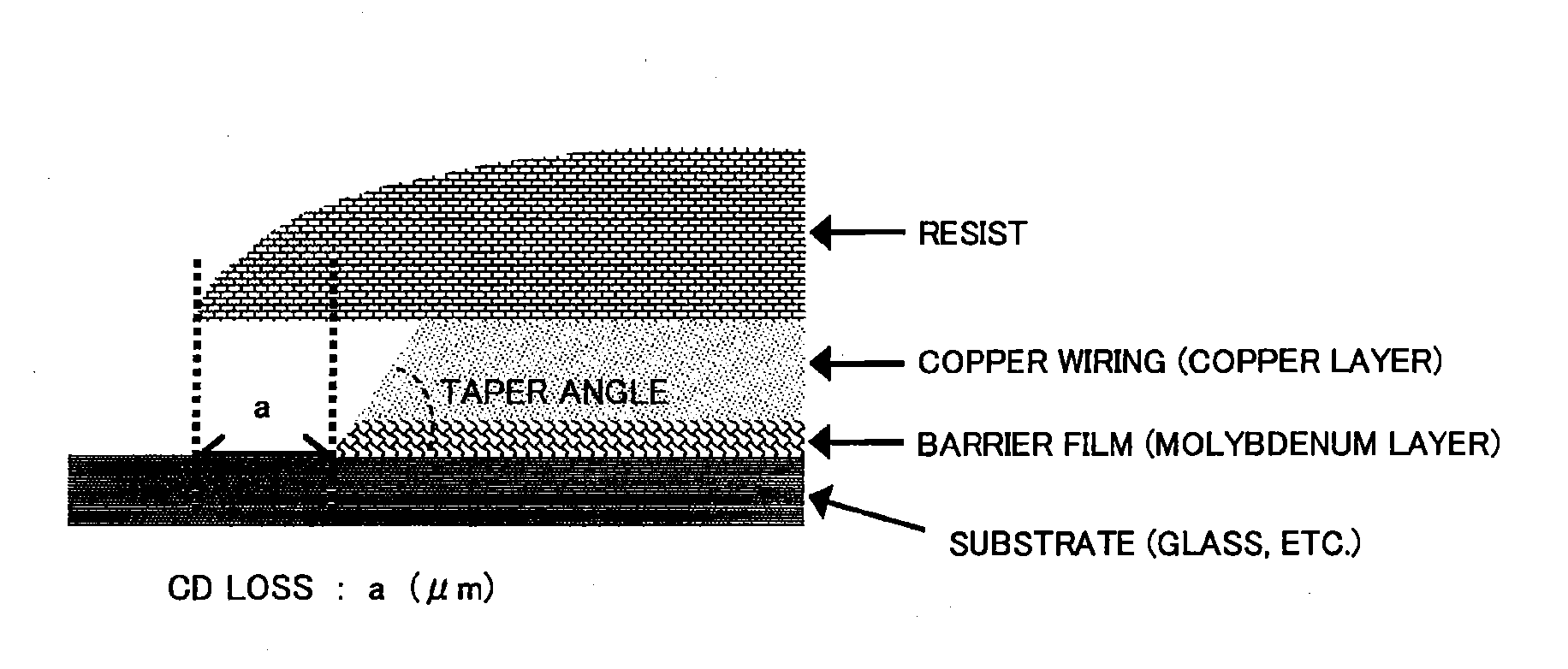
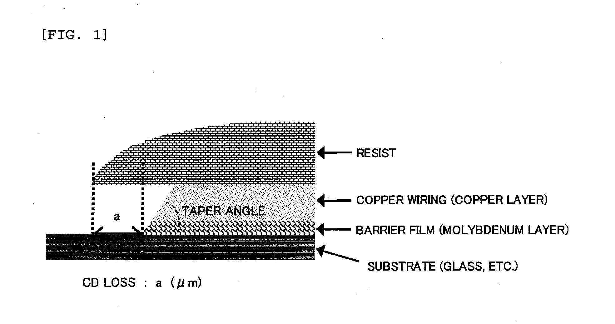
[0042]A sample of the etched multilayer thin film containing a copper layer and a molybdenum layer, as obtained in Examples and Comparative Examples, was cut and observed with a 30000 magnification through scanning electronic microscope (“S5000H

[0043]Type (Model Number)”, by Hitachi) (acceleration voltage 2 kV, acceleration current 10 μA). On the thus-taken SEM image, the taper angle and the CD loss (μm) as shown in FIG. 1 were determined.

[0044]When the taper angle and the CD loss (μm) fell within the standard ranges shown in Table 1, the sample was considered to be acceptable for the etching performance.

(Evaluation of Etching Residue)

[0045]A surface of a multilayer...

examples 1 to 5

[0050]The multilayer thin film having a copper layer and a molybdenum layer as obtained in the Fabrication Example was repeatedly subjected to an operation of etching with an etching solution shown in Table 2 at 35° C. by means of shower spraying; and with respect to the obtained multilayer thin film having a copper layer and a molybdenum layer after etching, a taper angle and a CD loss (μm) were obtained in a low-concentration region of a copper ion concentration in the etching solution (also expressed as “Cu concentration”) (from 200 to 1,000 ppm; also expressed as “low Cu concentration region”) and a high-concentration region of a copper ion concentration in the etching solution (from 3,000 to 4,000 ppm; also expressed as “high Cu concentration region”) by means of SEM observation.

[0051]Also, a time at which an etching subject of an area where the resist had not been patterned was determined to be etched by means of visual inspection was set up as a just etching time; and a time ...

examples 6 and 7

[0052]As Examples 6 and 7, etching was performed in the same manner as that in Example 4, except that in Example 4, a copper powder was previously added in a copper ion concentration of 200 ppm and 6,000 ppm, respectively to the Etching Solution 4 to be used. A taper angle, a CD loss (μm), and evaluation of residue of the multilayer thin film having a copper layer and a molybdenum layer contained therein, as obtained in the first etching are shown in Table 3. Also, a taper angle, a CD loss (μm), and evaluation of residue of the multilayer thin film having a copper layer and a molybdenum layer of Example 4 as obtained in the first etching are shown in Table 3.

TABLE 3Example4 (Firstetching)67Copper ion concentrationppm02006000Cu film thickness / Moangstrom / 5000 / 2005000 / 2005000 / 200film thicknessangstromJust etching timesec8080101Etching timesec120120120Taper angledegree354030CD lossμm1.01.00.65Overall evaluation of wiring cross-AAAsectional shapeEvaluation of residueBAAEvaluation of crys...


PUM

PropertyMeasurementUnit
taper angleaaaaaaaaaa
distanceaaaaaaaaaa
distanceaaaaaaaaaa

Abstract

Discloses are an etching solution for a multilayer thin film having a copper layer and a molybdenum layer contained therein; and an etching method of a multilayer thin film having a copper layer and a molybdenum layer contained therein using the same. Specifically disclosed are an etching solution for a multilayer thin film having a copper layer and a molybdenum layer contained therein, which includes (A) hydrogen peroxide, (B) a fluorine atom-free inorganic acid, (C) an organic acid, (D) an amine compound having a carbon number of from 2 to 10 and having an amino group and a hydroxyl group in a total group number of 2 or more, (E) an azole, and (F) a hydrogen peroxide stabilizer, and which has a pH of from 2.5 to 5; and an etching method using the same.

Description

TECHNICAL FIELD[0001]The present invention relates to an etching solution for a multilayer thin film having a copper layer and a molybdenum layer contained therein. In particular, the etching solution of the present invention is favorably used for etching a multilayer thin film having a copper layer is provided on a molybdenum layer.BACKGROUND ART[0002]Heretofore, aluminium or an aluminium alloy has been generally used as the wiring material for display devices such as flat panel displays, etc. However, with growing in size and increasing in resolution of displays, there has occurred a problem of RC delay caused by the characteristics such as the wiring resistance of such aluminium-based wiring materials and uniform panel displaying has tended to be difficult.[0003]Given the situation, the recent tendency is toward investigation of employing copper or copper-based wiring with a material having a lower resistance. However, copper has an advantage in that its resistance is low but, on...

Claims


Application Information

Patent Timeline
Patent Type & Authority Applications(United States)
IPC IPC(8): C23F1/10
CPCC23F1/18C23F1/26C23F1/44H01L21/32134H01L2924/0002H01L23/53238H01L2924/00C23F1/30H01L21/308H01L21/3205
Inventor OKABE, SATOSHINARITA, KAZUYOMATSUBARA, MASAHIDEADANIYA, TOMOYUKIMARUYAMA, TAKETO
Owner MITSUBISHI GAS CHEM CO INC
Why Eureka
Try Eureka