Single-sided light-actuated microfluidic device with integrated mesh ground

a microfluidic device and light-actuated technology, applied in the field of single-sided optoelectrowetting devices with integrated mesh ground, can solve the problems of affecting the electrowetting surface, affecting the flow rate of liquids, and complicating the introduction of droplets

Active Publication Date: 2016-06-09
BERKELEY LIGHTS +1
View PDF6 Cites 68 Cited by
  • Summary
  • Abstract
  • Description
  • Claims
  • Application Information

AI Technical Summary

Benefits of technology

This patent describes how to move small amounts of liquid on a special device called an SSOEW. The movement is controlled by shining laser light onto the device's surface while adjusting its position. This causes changes in the way the liquid interacts with the device, which results in the creation of patterns where the liquid moves around. These movements are possible because the device has certain properties that make it easier for liquids to stick to it than other surfaces.

Problems solved by technology

The technical problem addressed in this patent is how to improve microfluidic devices used for processing micro-objects like cells by making them easier to access through changes in the wettability of the electrowetting surface. This would allow for simpler addition and removal of droplets without requiring complicated hardware configurations.

Method used


Image

  • Single-sided light-actuated microfluidic device with integrated mesh ground
  • Single-sided light-actuated microfluidic device with integrated mesh ground
  • Single-sided light-actuated microfluidic device with integrated mesh ground

Examples


example 1

Movement of Water Droplets on a SSOEW-Configured Substrate

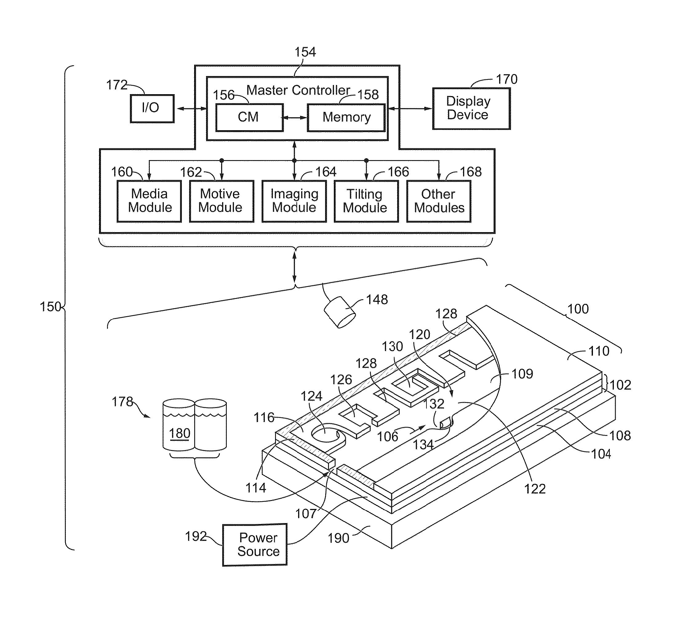
[0185]The movement of a 1 microliter droplet of water (conductivity 10 mS / m) was successfully demonstrated on the device of FIG. 1. The device featured a gold mesh ground that had a thickness of substantially 50 nm. Individual wires of the mesh had a width of substantially 10 microns and pitch of substantially 2 mm (β=0.5%). Prior to operation, the surface of the device was primed with silicone oil to reduce friction.

[0186]An AC voltage bias was applied between the ITO electrode and the mesh ground electrode. Structured light was then projected onto the substrate proximal to the droplet being moved, such that the light at least partially contacted the droplet. Droplets were successfully moved by shifting the location of the structured light. In this experiment, light having a square shape roughly the same size as the droplet was used. A maximum velocity of 0.33 cm / s was measured using a 40 ppV bias at 10 kHz.

[0187]The experim...

example 2

Movement of PBS Droplets on a SSOEW-Configured Substrate

[0188]Subsequently, a SSOEW-configured substrate was built having a photoconductive layer of substantially 1 micron thickness, a first dielectric layer of substantially 150 nm thickness, a second dielectric layer of substantially 2.5 nm in thickness, a mesh electrode having wires consisting of a gold layer of substantially 25 nm in thickness with an underlying titanium layer of substantially 10 nm in thickness, and a hydrophobic coating comprising a monolayer of octadecyltrimethoxysilane. The photoconductive layer consisted essentially of hydrogenated amorphous silicon (a-Si:H), and the first and second dielectric layers were made from Alumina (i.e., aluminum oxide deposited by ALD). The mesh electrode was interposed between the first and second dielectric layers, and the wires of the mesh electrode were substantially 10 microns in width, with a pitch of approximately 300 microns.

[0189]A droplet of PBS (approximately 1.5 microl...


PUM


Abstract

Single-sided optoelectrowetting (SSOEW)-configured substrates are provided, as well as microfluidic devices that include such substrates. The substrates can include a planar electrode, a photoconductive (or photosensitive) layer, a dielectric layer (single-layer or composite), a mesh electrode, and a hydrophobic coating. Fluid droplets can be moved across the hydrophobic coating of such substrates in a light-actuated manner, upon the application of a suitable AC voltage potential across the substrate and the focusing of light into the photoconductive layer of the substrate in a location proximal to the droplets. Walls can be disposed upon the substrates to form the microfluidic devices. Together the walls and substrate can form a microfluidic circuit, through which droplets can be moved.

Description


Claims


Application Information

Patent Timeline
Owner BERKELEY LIGHTS
Why Eureka
Try Eureka