Organic light-emitting display and method of driving the same

a technology of light-emitting display and organic light-emitting display, which is applied in the direction of electric digital data processing, instruments, computing, etc., can solve the problems of reducing image quality, and achieve the effect of accurate measurement of the electric current of each pixel, simple structure and reduced memory siz

Inactive Publication Date: 2016-06-09
SAMSUNG DISPLAY CO LTD
View PDF9 Cites 45 Cited by
  • Summary
  • Abstract
  • Description
  • Claims
  • Application Information

AI Technical Summary

Benefits of technology

[0008]Embodiments of the present invention provide an organic light-emitting display which can accurately measure an electric current of each pixel using a simple structure and relatively reduce a memory size.
[0009]Embodiments of the present invention also provide a method of driving an organic light-emitting display which can accurately measure an electric current of each pixel using a simple structure and reduce a memory size.
[0022]The first measurement circuit may include a first integrator circuit which measures current characteristics of an organic light-emitting diode in a pixel receiving the reference voltage from the first measurement circuit, during the measurement period, a first amplifier which amplifies an output signal of the first integrator circuit and a first CDS which removes noise from an output signal of the first amplifier, and the second measurement circuit includes a second integrator circuit which measures current characteristics of an organic light-emitting diode in a pixel receiving the reference voltage from the second measurement circuit, during the measurement period, a second amplifier which amplifies an output signal of the second integrator circuit and a second CDS which removes noise from an output signal of the second amplifier.

Problems solved by technology

If the luminance imbalance worsens, an image sticking phenomenon may occur, resulting in reduced image quality.

Method used


Image

  • Organic light-emitting display and method of driving the same
  • Organic light-emitting display and method of driving the same
  • Organic light-emitting display and method of driving the same

Examples


Embodiment Construction

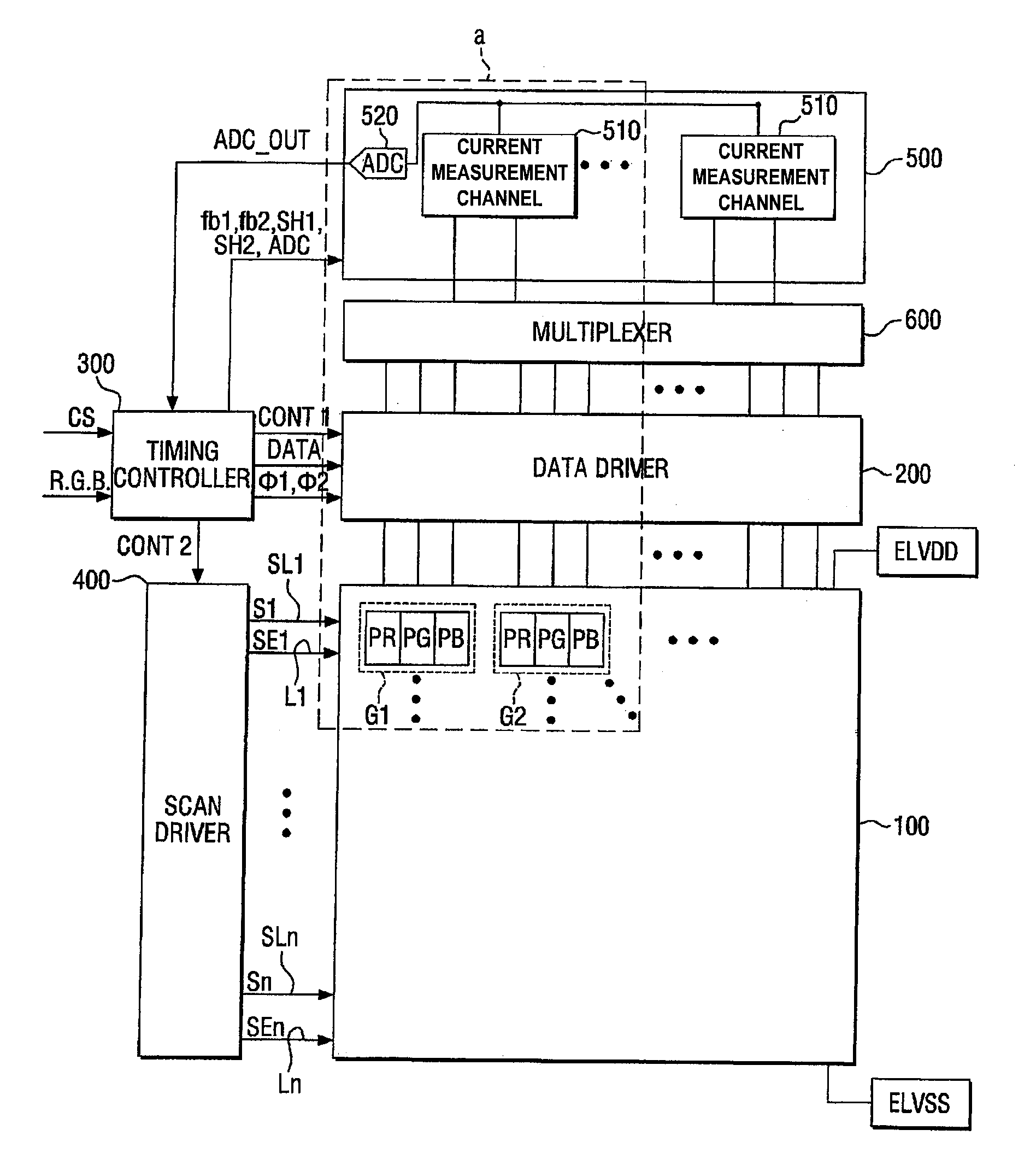
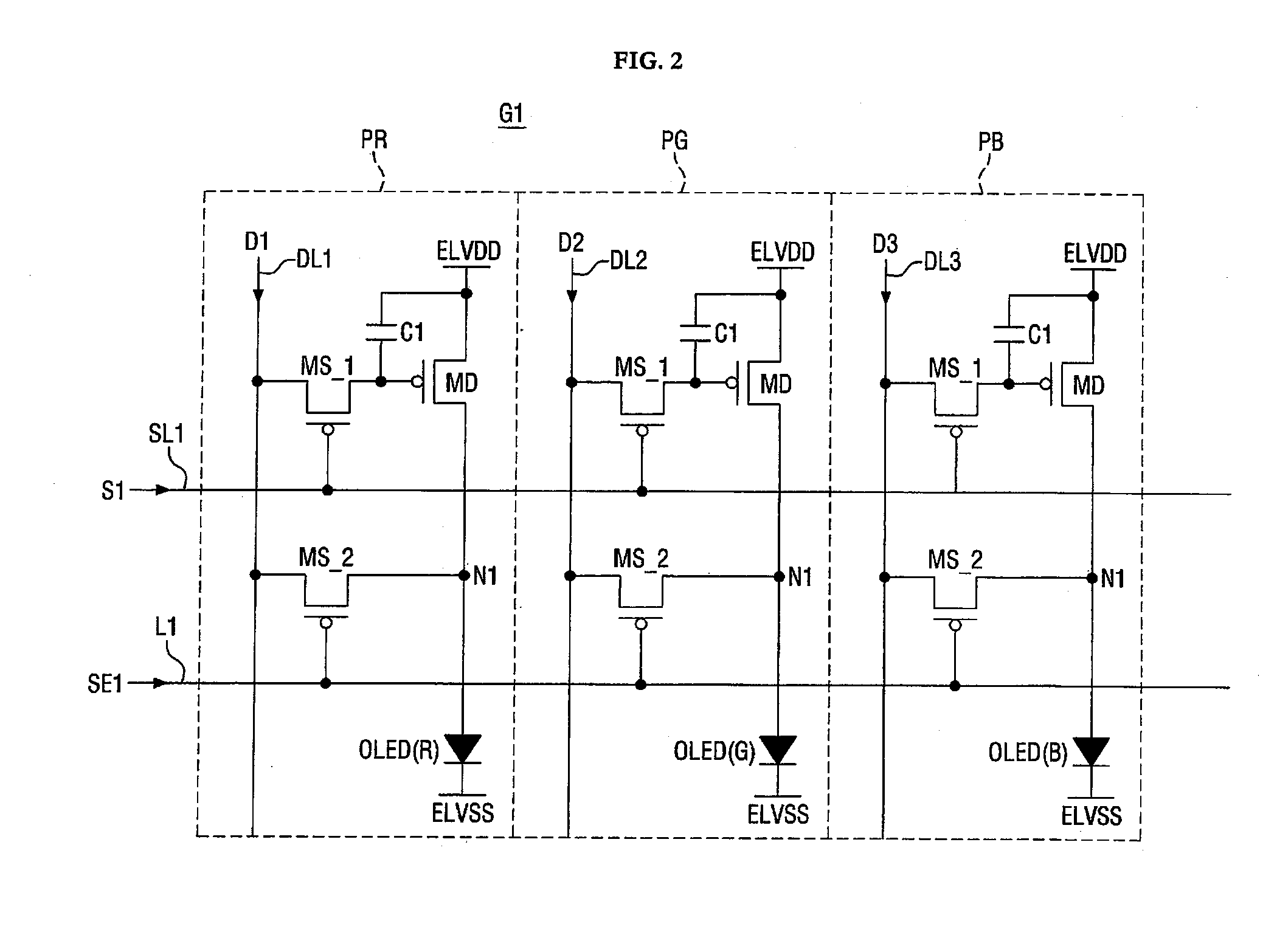
[0041]Features of embodiments of the present invention and methods of accomplishing the same may be understood more readily by reference to the following detailed description of preferred embodiments and the accompanying drawings. The present invention may, however, be embodied in many different forms and should not be construed as being limited to the embodiments set forth herein. Rather, these embodiments are provided so that this disclosure will be thorough and complete and will fully convey the concept of the invention to those skilled in the art, and the present invention will only be defined by the appended claims and their equivalents. Like reference numerals refer to like elements throughout the specification.

[0042]The terminology used herein is for the purpose of describing particular embodiments only and is not intended to be limiting of the invention. As used herein, the singular forms “a” and “an” are intended to include the plural forms as well, unless the context clear...


PUM


Abstract

An organic light-emitting display devices includes a display panel having first and second pixel groups, each group including first, second, and third pixels which emit light of different colors and a current measurement unit having a plurality of current measurement channels connected to the first and second pixel groups by data lines, wherein each of the current measurement channels includes a first measurement circuit connected to one of the first, second, and third pixels in the first pixel group and measures current characteristics of the connected one of the pixels and a second measurement circuit which measures current characteristics of one of the first, second, and third pixels, in the second pixel group, which emits light of the same color as that of light emitted from the one of the pixels connected to the first measurement circuit.

Description

CROSS-REFERENCE TO RELATED APPLICATION[0001]This application claims priority to and the benefit of Korean Patent Application No. 10-2014-0171982 filed on Dec. 3, 2014 in the Korean Intellectual Property Office, the disclosure of which is incorporated herein by reference in its entirety.BACKGROUND[0002]1. Field[0003]Embodiments of the present invention relate to an organic light-emitting display and a method of driving the same.[0004]2. Description of the Related Art[0005]An organic light-emitting display, which is drawing attention as a next-generation display, displays an image using organic light-emitting diodes which emit light by recombination of electrons and holes. The organic light-emitting display has features of high response speed, high luminance, a wide viewing angle, and low power consumption.[0006]The organic light-emitting display controls the amount of current provided to the organic light-emitting diodes using a driving transistor included in each pixel and generates...

Claims


Application Information

Patent Timeline
Patent Type & Authority Applications(United States)
IPC IPC(8): G09G3/32G09G3/20
CPCG09G3/325G09G3/2003G09G3/3283G09G3/3291G09G2310/0297G09G2310/0291G09G2300/043G09G2310/0272G09G2300/0819G09G3/3233G09G2300/0866G09G2320/0233G09G2320/029G09G2320/0295G09G2320/043G09G2350/00H10K59/84H10K59/00H10K71/00
Inventor KIM, BO YEONKWON, OH JO
Owner SAMSUNG DISPLAY CO LTD
Why Eureka
Try Eureka