Semiconductor device

Inactive Publication Date: 2005-08-04
SEMICON ENERGY LAB CO LTD
View PDF51 Cites 28 Cited by
  • Summary
  • Abstract
  • Description
  • Claims
  • Application Information

AI Technical Summary

Benefits of technology

[0052] According to the invention, a feedback circuit is formed by using an amplifier circuit, thereby a transistor is controlled. Thus, the transistor can output a constant current without being affected by a variation. In the case of setting in this manner, a set operation can be performed rapidly since an amplifier circuit is

Problems solved by technology

However, a parasitic capacitance of a wiring used for supplying a signal current to a driving TFT and a light emitting element is quite large, therefore, a time constant for charging the parasitic capacitance of the wiring becomes large when the signal current is smal

Method used


Image

  • Semiconductor device
  • Semiconductor device
  • Semiconductor device

Examples


embodiment mode 1

[0230] According to the invention, a pixel is formed by an element which is capable of controlling a luminance according to a current value supplied to a light emitting element. Typically, an EL element can be applied. There are various structures of an EL element, however, any element structure can be applied to the invention as long as it can control a luminance according to the current value. That is, an EL element is formed by freely combining a light emitting layer, a charge transporting layer, or a charge injection layer. A low molecular weight organic material, a medium molecular weight organic material (that does not have subliming property and that has 20 or less of molecules, or a length of chained molecules of 10 μm or less) and a high molecular weight organic material may be used as materials for forming the EL element. Further, materials those an inorganic material is mixed or dispersed with these materials may be used.

[0231] Moreover, the invention can be applied not ...

embodiment mode 2

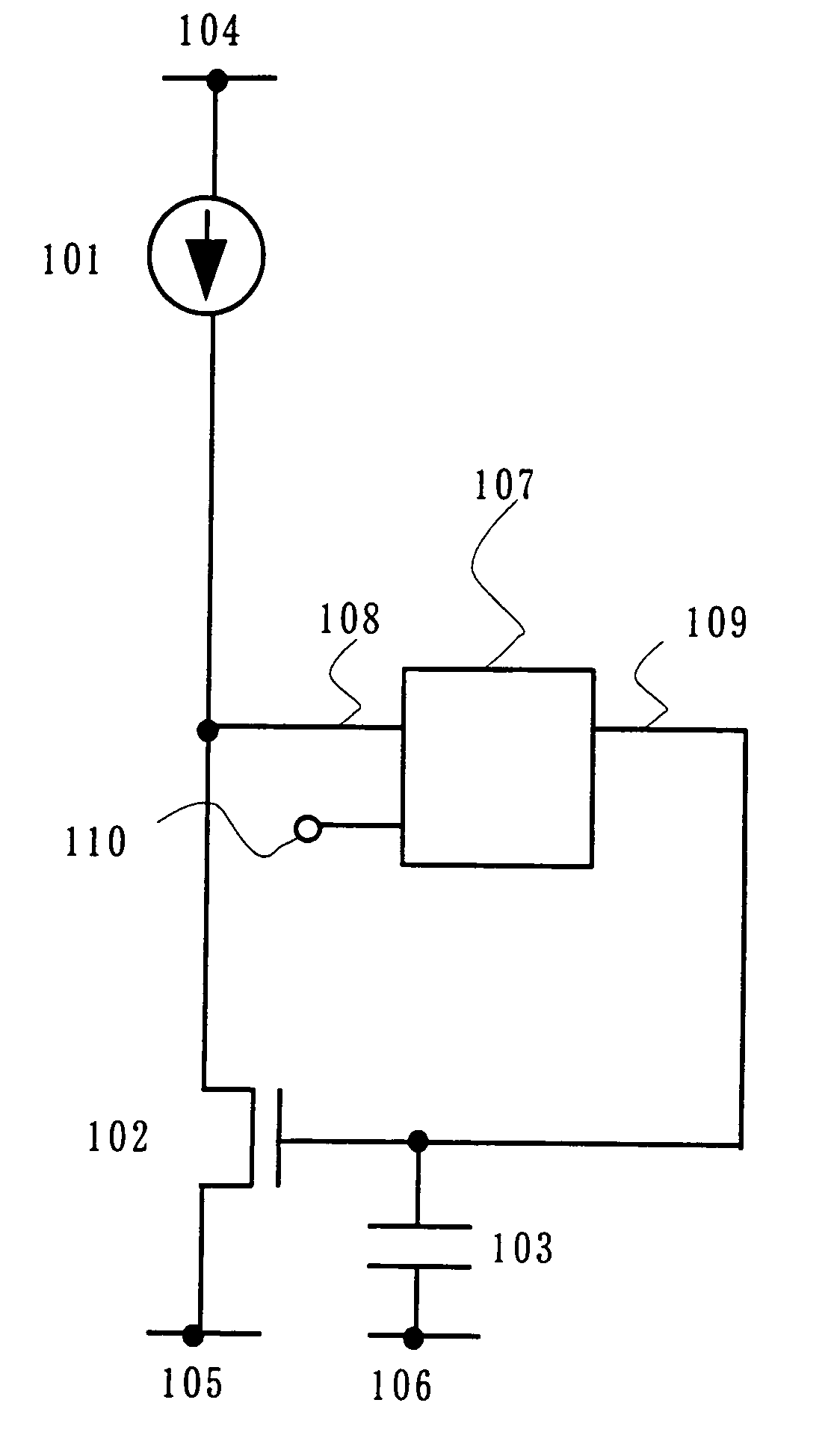
[0255] In Embodiment Mode 2, an example of an amplifier circuit used in FIGS. 1 to 3 is described.

[0256] First, an operational amplifier is taken as an example of an amplifier circuit. FIG. 4 shows a configuration diagram corresponding to FIG. 1 as the case of using an operational amplifier as an amplifier circuit. The first input terminal 108 of the amplifier circuit 107 corresponds to a non-inverting (positive) input terminal while the second input terminal 110 corresponds to an inverting input terminal of the operational amplifier 407.

[0257] An operational amplifier normally operates so that a potential of a non-inverting (positive) input terminal and a potential of an inverting input terminal become equal to each other. Therefore, in the case of FIG. 4, the gate potential of the current source transistor 102 is controlled so that a drain potential of the current source transistor 102 and a potential of the inverting input terminal become equal to each other. Therefore, in the ...

embodiment mode 3

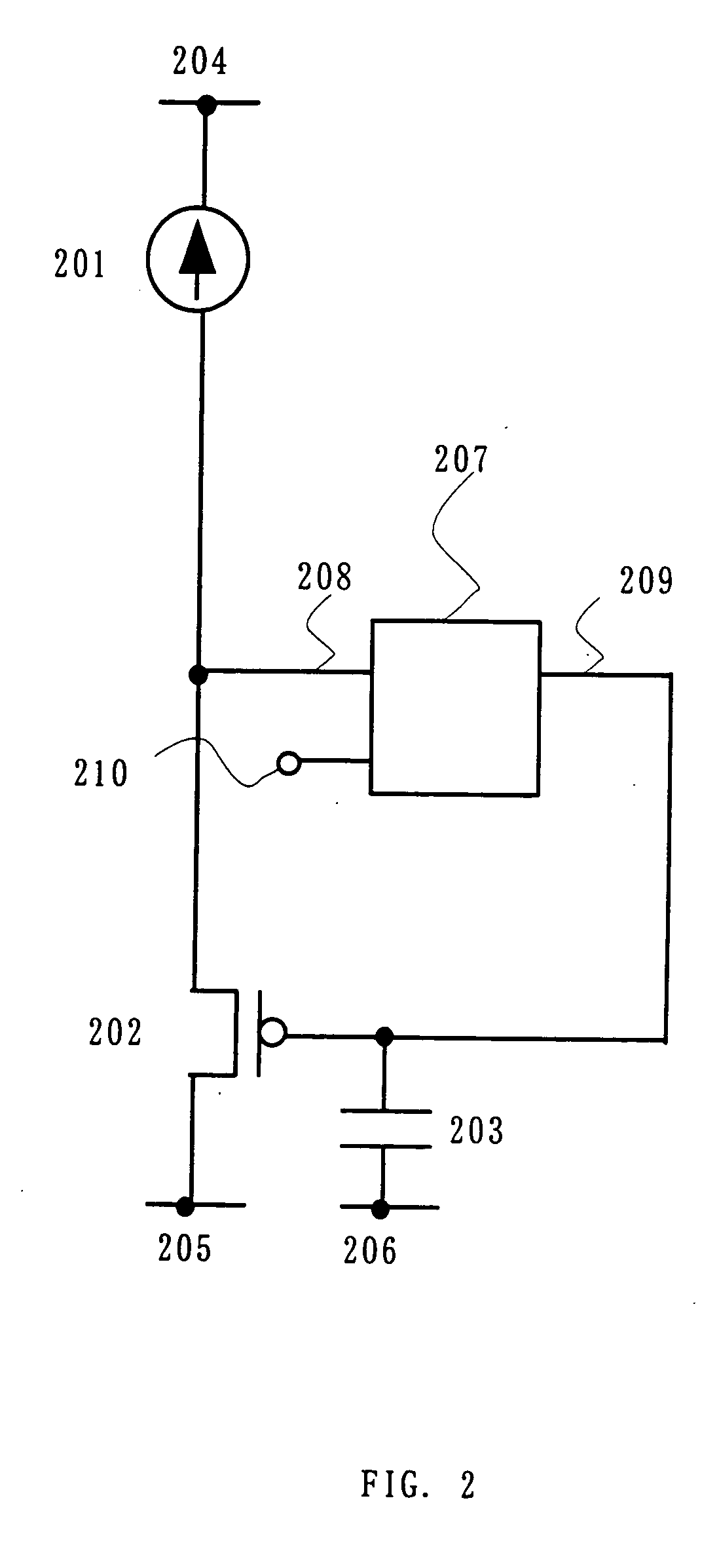
[0267] The invention is set so that the current source transistor can flow the current Idata by flowing the current Idata from the current source circuit. Then, the current source transistor which is set operates as a current source circuit to supply a current to various loads. In this embodiment mode, a connecting structure of a load and a current source transistor, a structure of a transistor when supplying a current to a load and the like are described.

[0268] Note that in this embodiment mode, the configuration of FIG. 1, a configuration using an operational amplifier as an amplifier circuit (FIG. 4) and the like are referred for description, however, the invention is not limited to this and can be applied to other configurations described in FIGS. 2 to 8.

[0269] Further, the case of flowing a current from the current source circuit to the current source transistor which is an N-channel type transistor is described, however, the invention is not limited to this and can be applie...


PUM


Abstract

A semiconductor device is provided in which a transistor which supplies a current to a load (an EL pixel and a signal line) can supply an accurate current without being affected by a variation. A voltage of each terminal of a transistor is controlled by using a feedback circuit using an amplifier circuit. A current Idata is inputted from a current source circuit to a transistor and a gate-source voltage (a source potential) required for the transistor to flow the current Idata is set by using the feedback circuit. The feedback circuit is controlled to operate so that a drain potential of the transistor becomes a predetermined potential. Then, a gate voltage required to flow the current Idata is set. By using the set transistor, an accurate current can be supplied to the load (an EL element and a signal line). As a drain potential can be controlled, the kink effect can be reduced.

Description

TECHNICAL FIELD [0001] The present invention relates to a semiconductor device provided with a function to control by a transistor a current to be supplied to a load. More particularly, the invention relates to a semiconductor device including a pixel formed of a current drive type light emitting element of which luminance changes according to current, and a signal line driver circuit which drives a pixel. BACKGROUND ART [0002] In a display device using a self-light emitting type light emitting element represented by an organic light emitting diode (also referred to as an OLED (Organic Light Emitting Diode), an organic EL element, an electroluminescence (EL) element and the like), a passive matrix method and an active matrix method are known as its driving method. The former has a simple structure, but has a problem such that a realization of a large and high definition display is difficult. Therefore, the active matrix method is actively developed in recent years in which a current...

Claims


Application Information

Patent Timeline
IPC IPC(8): G09G3/32
CPCG09G3/3241G09G3/325G09G3/3283G09G2320/0233G09G2300/0861G09G2310/027G09G2300/0842
Inventor KIMURA, HAJIME
Owner SEMICON ENERGY LAB CO LTD
Why Eureka
Try Eureka