Semiconductor device

a technology of semiconductor devices and circuits, applied in the direction of instruments, light sources, machine control, etc., can solve the problems of increasing the capacitance of wirings, slow signal writing speed, and large parametric capacitance of wirings used for supplying signal current to driving tft and light emitting elements, so as to achieve the effect of quick set operation

Inactive Publication Date: 2005-03-17
SEMICON ENERGY LAB CO LTD
View PDF37 Cites 28 Cited by
  • Summary
  • Abstract
  • Description
  • Claims
  • Application Information

AI Technical Summary

Benefits of technology

[0046] According to the invention, a feedback circuit is constituted by an amplifier circuit in order to control a transistor. As a result, the transistor can output a constant current without being influenced by variations. Such a set operation can be carried out quickly since the amplifier circuit is used. Thus, an accurate current can be output in an output operation. In addition, the amplifier circuit allows a set operation to be carried out with accuracy even when current characteristics vary. Therefore, the amplifier circuit can be easily constituted by transistors such as TFTs with large variations in current characteristics.

Problems solved by technology

However, parasitic capacitance of a wiring used for supplying a signal current to a driving TFT and a light emitting element is considerably large.
Therefore, there are problems in that in the case of a signal current being small, the time constant for charging parasitic capacitance of a wiring is increased, and thereby signal writing speed becomes slower.
That is, the problem is that it takes a long time to develop at a gate terminal a voltage required for flowing a signal current supplied to a transistor, and signal writing speed becomes slower.
In addition, as seen by comparison of FIG. 44 and FIG. 6, the circuit in FIG. 44 has much more transistors and a more complicated configuration.
Accordingly, reduced productive yield, increased cost, enlarged layout of circuit, and increased power consumption may occur.

Method used


Image

  • Semiconductor device
  • Semiconductor device
  • Semiconductor device

Examples


embodiment

[0092] (Embodiment Mode 1)

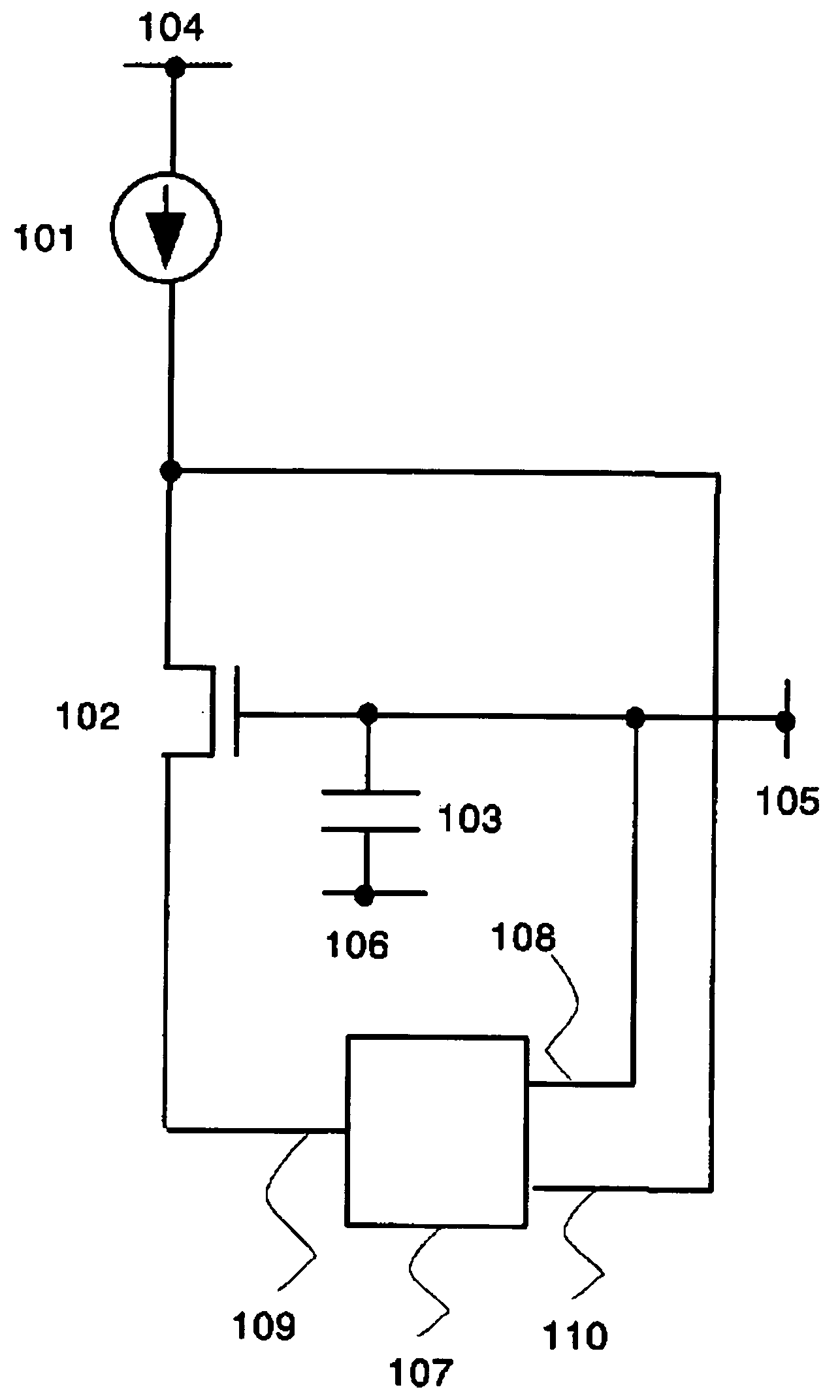
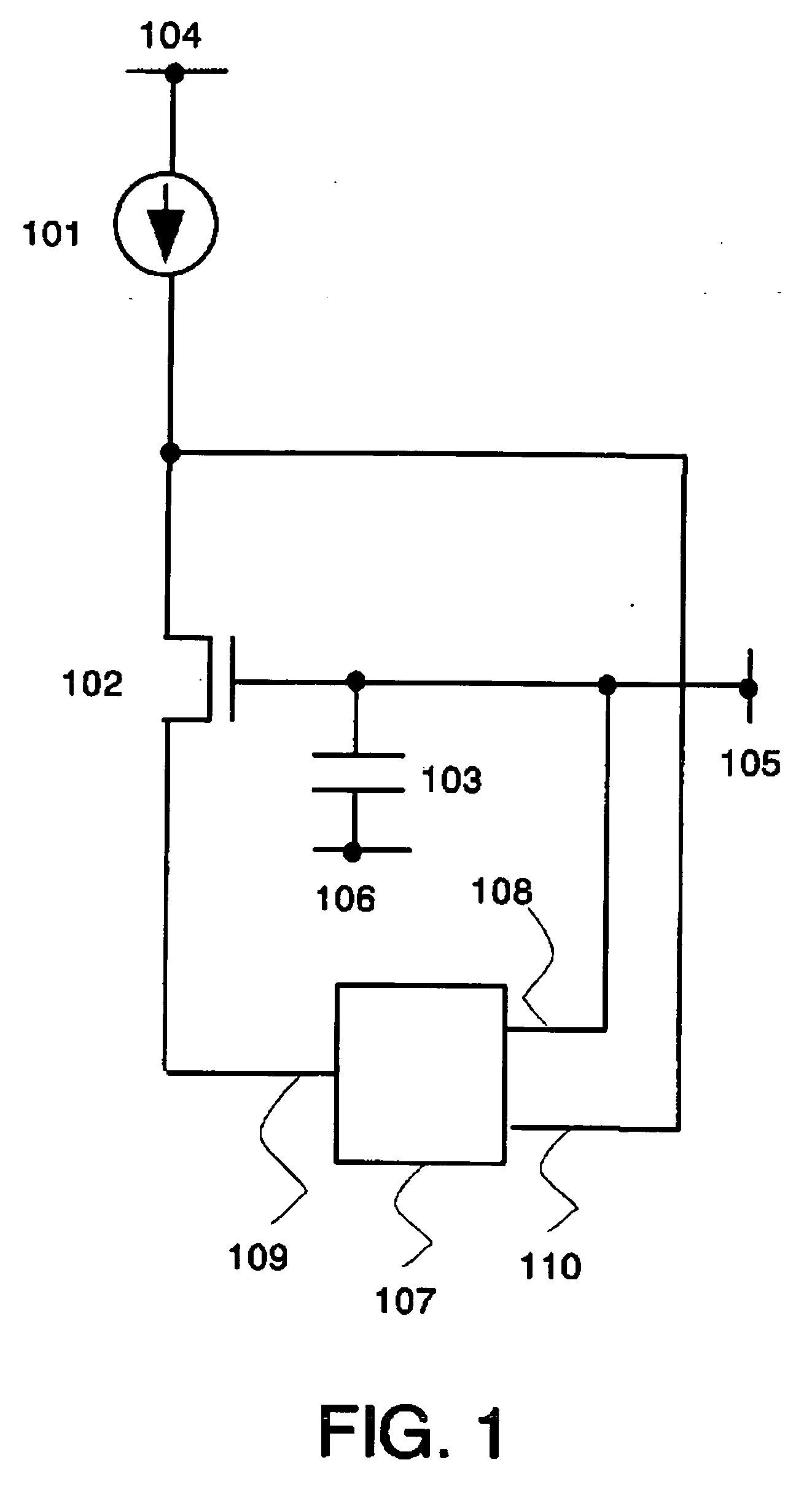
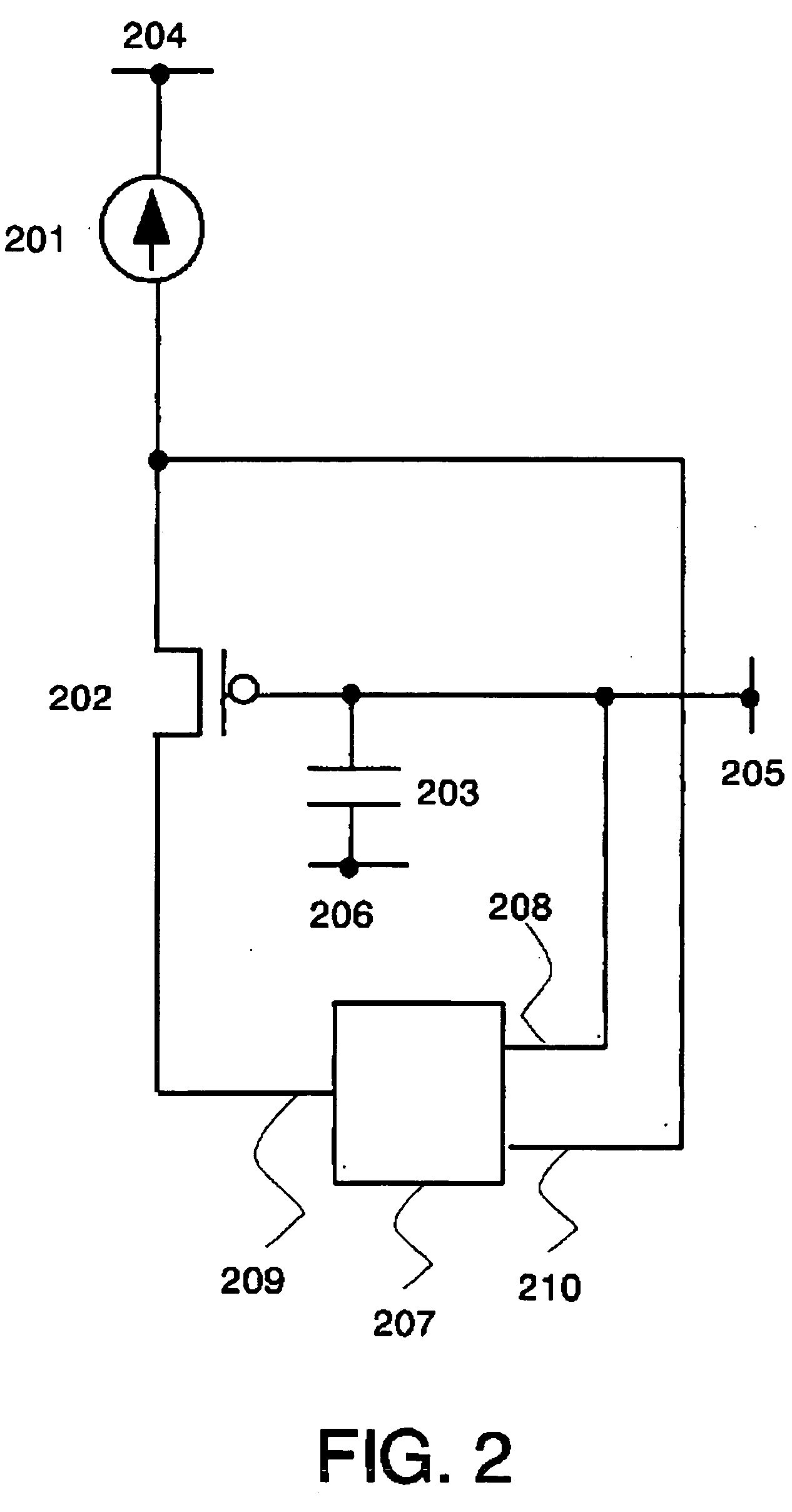
[0093] According to the invention, a pixel comprises an element whose luminance can be controlled by a current value flowing into a light emitting element. Typically, an EL element can be adopted. Although various configurations of an EL element are known, any configuration of an EL element can be used in the invention as long as the luminance can be controlled by a current value. In other words, an EL element may be formed by freely combining a light emitting layer, an electron transporting layer, or an electron injection layer. As a material for forming an EL element, a low molecular weight organic material, a medium molecular weight organic material (an organic light emitting material that does not have subliming property and that has a molecular number of 20 or less, or a length of chained molecules of 10 μm or less), or a high molecular weight organic material may be employed. Alternatively, an inorganic material may be mixed or dispersed into these or...


PUM


Abstract

A semiconductor device in which a transistor can supply an accurate current to a load (EL pixel and signal line) without being influenced by variations is provided. A voltage at each terminal of a transistor is adjusted by a feedback circuit using an amplifier circuit. A current Idata is input from a current source circuit to the transistor, and a gate-source voltage is set by the feedback circuit so that the transistor can flow the current Idata. The feedback circuit controls the transistor to operate in a saturation region. Thus, a gate voltage required for flowing the current Idata is set. With the use of the set transistor, a current can be supplied to a load (EL pixel and signal line) with accuracy. Note that a desired gate voltage can be set quickly since the amplifier circuit is utilized.

Description

TECHNICAL FIELD [0001] The present invention relates to a semiconductor device provided with a function for controlling a current supplied to a load by a transistor. In particular, the invention relates to a semiconductor device that includes a pixel having a current-driven light emitting element whose luminance varies depending on a current and a signal line driver circuit for driving the pixel. BACKGROUND ART [0002] In recent years, a so-called self luminous type display device that includes a pixel having a light emitting element such as a light emitting diode (LED) attracts attention. As a light emitting element used for such a self luminous type display device, an organic light emitting diode (also called an OLED, an organic EL element, an electro luminescence (EL) element, or the like) draws attention and has been used for an organic EL display and the like. [0003] Since a light emitting element such as an OLED is self luminous type, it does not require a backlight, and has th...

Claims


Application Information

Patent Timeline
Patent Type & Authority Applications(United States)
IPC IPC(8): G05F3/24
CPCG05F3/242G09G3/3233G09G2300/0809G09G2300/0833G09G2320/043G09G2300/0861G09G2310/0251G09G2320/0295G09G2300/0842
Inventor KIMURA, HAJIME
Owner SEMICON ENERGY LAB CO LTD
Why Eureka
Try Eureka