Method for manufacturing a liquid crystal panel

a liquid crystal display and manufacturing method technology, applied in the manufacture of electrode systems, electric discharge tubes/lamps, instruments, etc., can solve the problems of large design difficulty of liquid crystal displays and mura defects

Active Publication Date: 2016-06-23
SHENZHEN CHINA STAR OPTOELECTRONICS TECH CO LTD
View PDF0 Cites 7 Cited by
  • Summary
  • Abstract
  • Description
  • Claims
  • Application Information

AI Technical Summary

Benefits of technology

[0006]An object of the present invention is to provide a method of manufacturing a liquid crystal panel, where a liquid crystal cell having non-uniform gaps can be prevented, so as to solve the technical problem caused by a partial gaps of the liquid crystal cell becoming smaller, thereby generating mura defects when bonding driver chips in the conventional method of manufacturing the liquid crystal panel.

Problems solved by technology

However, the design difficulty of the liquid crystal panel is large.
However, the frame on the driver circuit side is near an effective display area (AA area) of the liquid crystal panel, so that a substrate glass of the AA area expands by heat due to a partial temperature is too high when bonding the driver chips, so as to protrude toward an inner side of the liquid crystal panel.
Thus, a gap of a liquid crystal cell on the region where expands by heat becomes smaller, and mura defects are generated.

Method used


Image

  • Method for manufacturing a liquid crystal panel
  • Method for manufacturing a liquid crystal panel
  • Method for manufacturing a liquid crystal panel

Examples


Embodiment Construction

[0077]The following embodiments refer to the accompanying drawings for exemplifying specific implementable embodiments of the present invention. Furthermore, directional terms described by the present invention, such as upper, lower, front, back, left, right, inner, outer, side, etc., are only directions by referring to the accompanying drawings, and thus the used directional terms are used to describe and understand the present invention, but the present invention is not limited thereto.

[0078]In the drawings, the same reference symbol represents the same or a similar component.

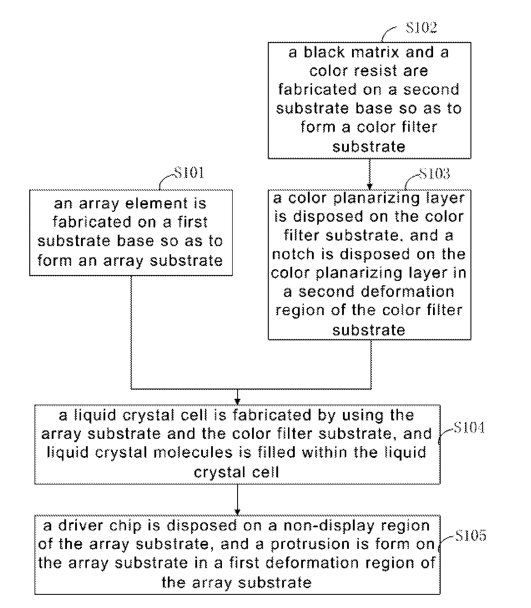
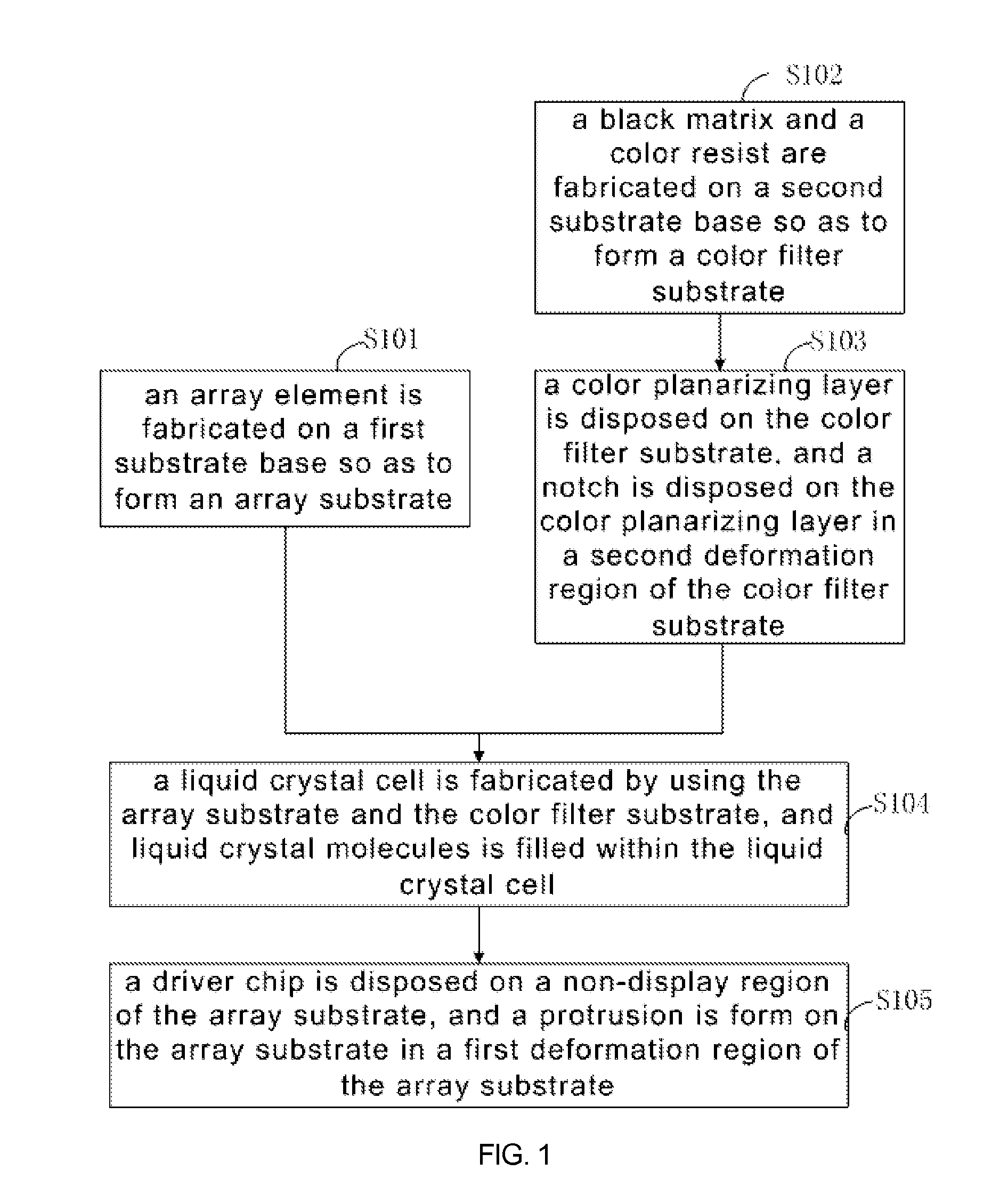
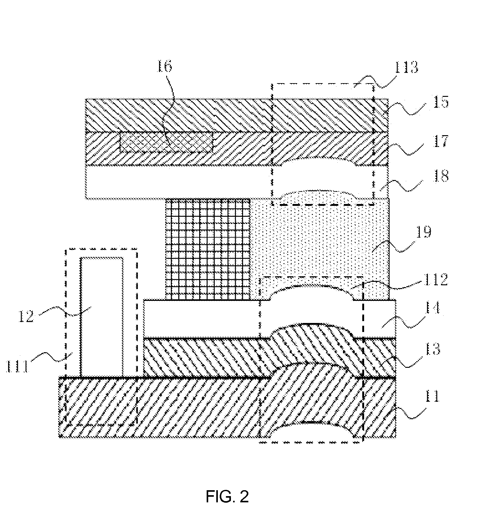
[0079]Please refer to FIG. 1 and FIG. 2, FIG. 1 is a flow chart of a method of manufacturing a liquid crystal panel of a first preferred embodiment of the present invention, and FIG. 2 is a schematic diagram showing a structure formed after the step S105 of the method of manufacturing the liquid crystal panel of the first preferred embodiment of the present invention. In this preferred embodiment, the method ...


PUM

PropertyMeasurementUnit
depthaaaaaaaaaa
coloraaaaaaaaaa
depthaaaaaaaaaa

Abstract

A method of manufacturing the liquid crystal panel is provided, including: forming an array substrate; forming a color filter substrate; disposing a color planarizing layer on the color filter substrate, and disposing a notch on the color planarizing layer on the color filter substrate; fabricating a liquid crystal cell by using the array substrate and the color filter substrate, and filling liquid crystal molecules within the liquid crystal cell; and forming a on the array substrate in a first deformation region of the array substrate. The liquid crystal cell having non-uniform gaps is prevented.

Description

FIELD OF THE INVENTION[0001]The present invention relates to a field of liquid crystal displays, and particularly to a method of manufacturing a liquid crystal panel.BACKGROUND OF THE INVENTION[0002]With the development on technologies and the emergence of smartphones and tablets, it put forward a high specification requirement for the medium or small size liquid crystal panels. One of aspects is the liquid crystal panel with a narrow frame.[0003]Under the same display area, a non-display region on the edge of the liquid crystal panel can be decreased by using the narrow frame design, so that the liquid crystal panel has a small size. However, the design difficulty of the liquid crystal panel is large. For example, the space utilization of driver circuits should be increased. The frame outside a driver circuit side of the conventional middle-end and high-end liquid crystal panels is about 5 mm.[0004]However, the frame on the driver circuit side is near an effective display area (AA ...

Claims


Application Information

Patent Timeline
Patent Type & Authority Applications(United States)
IPC IPC(8): G02F1/1345G02F1/1362G02F1/1337G02F1/1341G02F1/1335
CPCG02F1/13454G02F1/1341G02F1/133512G02F2001/133357G02F1/1337G02F1/1362G02F1/133516G02F1/1333G02F1/133514G02F1/133357G02F1/133388
Inventor YE, YANXI
Owner SHENZHEN CHINA STAR OPTOELECTRONICS TECH CO LTD
Why Eureka
Try Eureka