Liquid-crystal display device comprising a depression formed on inner surface of a substrate for receiving excess liquid crystal
a liquid crystal display and depression technology, applied in non-linear optics, instruments, optics, etc., can solve problems such as problems, and achieve the effect of suppressing effective the formation of the slope area
- Summary
- Abstract
- Description
- Claims
- Application Information
AI Technical Summary
Benefits of technology
Problems solved by technology
Method used
Image
Examples
first embodiment
[0066]A LCD device according to a first embodiment of the invention has the structure shown in FIGS. 5 and 6.
[0067]FIG. 5 shows the state of the LCD device of the first embodiment in a step of its fabrication method. In FIG. 5, a TFT substrate member 12a and an opposite substrate member 14a are coupled to each other to simultaneously form two LCD panes 26. Thus, this method includes the two-panel formation step. The two panels 26 are located in the middle of the coupled substrate members 12a and 14a to be adjacent to each other. The liquid crystal layer is not yet formed between the members 12a and 14a at this state.
[0068]Each panel 26 comprises a rectangular display region 18 in which pixels and their TFTs are arranged in a matrix array, a sealing member 22 formed to define the outer edge of the LCD device, and a rectangular frame-shaped non-display region 20 formed between the outer edge of the display region 18 and the member 22. The width of the non-display region 20 is, for exa...
second embodiment
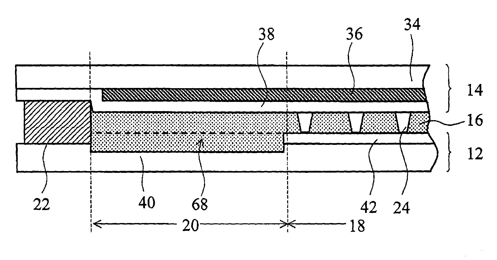
[0095]FIG. 9 shows a LCD device according to a second embodiment of the invention, which has the same structure as the device of the first embodiment shown in FIG. 6, except that a buffering space 68 is additionally formed in the gap between the TFT and opposite substrates 12 and 14. Therefore, the explanation about the same structure is omitted here for the sake of simplification by attaching the same reference symbols as those used in the first embodiment to the same or corresponding elements.
[0096]Since the device of the second embodiment has the same structure except for the space 68, it has not only the same advantages as those in the first embodiment but also an additional advantage that a uniform gap is easily obtainable between the substrates 12 and 14 in the whole device.
[0097]The buffering space 68 is used for receiving the extra liquid crystal confined in the inter-substrate gap. Thus, the gap is more likely to be uniform in the whole device compared with the first embodi...
third embodiment
[0118]FIG. 12 shows a LCD device according to a third embodiment of the invention, which has the same structure as the device of the first embodiment shown in FIG. 6, except that a buffering space 68 is additionally formed in the gap between the TFT and opposite substrates 12 and 14. The space 68 is realized by selectively removing the dielectric overcoat layer 38 on the opposite substrate 14, which is unlike the device of the second embodiment of FIG. 9.
[0119]Therefore, the explanation about the same structure is omitted here for the sake of simplification by attaching the same reference symbols as those used in the first embodiment to the same or corresponding elements.
[0120]Obviously, the device of the third embodiment has the same advantages as those of the second embodiment.
PUM
 Abstract
Description
Claims
Application Information


