Pixel and organic light emitting display device using the same

a technology of light-emitting display device and pixel, which is applied in the direction of static indicating device, cathode-ray/electron-beam tube circuit elements, instruments, etc., can solve the problems of image with a desired luminance not being displayed by leakage current, undesired image, etc., and achieve the effect of preventing deterioration of image quality

Active Publication Date: 2014-06-19
SAMSUNG DISPLAY CO LTD
View PDF16 Cites 34 Cited by
  • Summary
  • Abstract
  • Description
  • Claims
  • Application Information

AI Technical Summary

Benefits of technology

[0017]In the pixel and the organic light emitting display device according to the present invention, the gate electrode of the driving transistor is not coupled to a separate initialization power source, and accordingly, it is possible to the amount of leakage current. Further, the pixel of the present invention includes one capacitor, and thus it is possible to prevent deterioration of image quality due to a change in capacitance of the capacitor.

Problems solved by technology

However, in the organic light emitting display device, the amount of current that flows in an organic light emitting diode is changed depending on the variation in the threshold voltage of the driving transistor included in each pixel, and therefore, images with unequal luminance are displayed.
Practically, it is impossible in the current fabrication process to fabricate the organic light emitting display device so that all transistors of the organic light emitting display device have the same characteristics.
However, in a case where the gate electrode of the driving transistor is initialized using the initialization power source in the conventional method, an image with a desired luminance is not displayed by leakage current.
However, in a case where the two capacitors are included in the compensation circuit, an undesired image, e.g., a blurred image is displayed by a change in capacitance between the capacitors due to process tolerance.
If the capacitance of one of the two capacitors is increased, the predetermined ratio is not maintained, and accordingly, image quality is deteriorated.

Method used


Image

  • Pixel and organic light emitting display device using the same
  • Pixel and organic light emitting display device using the same
  • Pixel and organic light emitting display device using the same

Examples


Embodiment Construction

[0022]Hereinafter, certain exemplary embodiments according to the present invention will be described with reference to the accompanying drawings. Here, when a first element is described as being coupled to a second element, the first element may be not only directly coupled to the second element but may also be indirectly coupled to the second element via a third element. Further, some of the elements that are not essential to the complete understanding of the invention are omitted for clarity. Also, like reference numerals refer to like elements throughout.

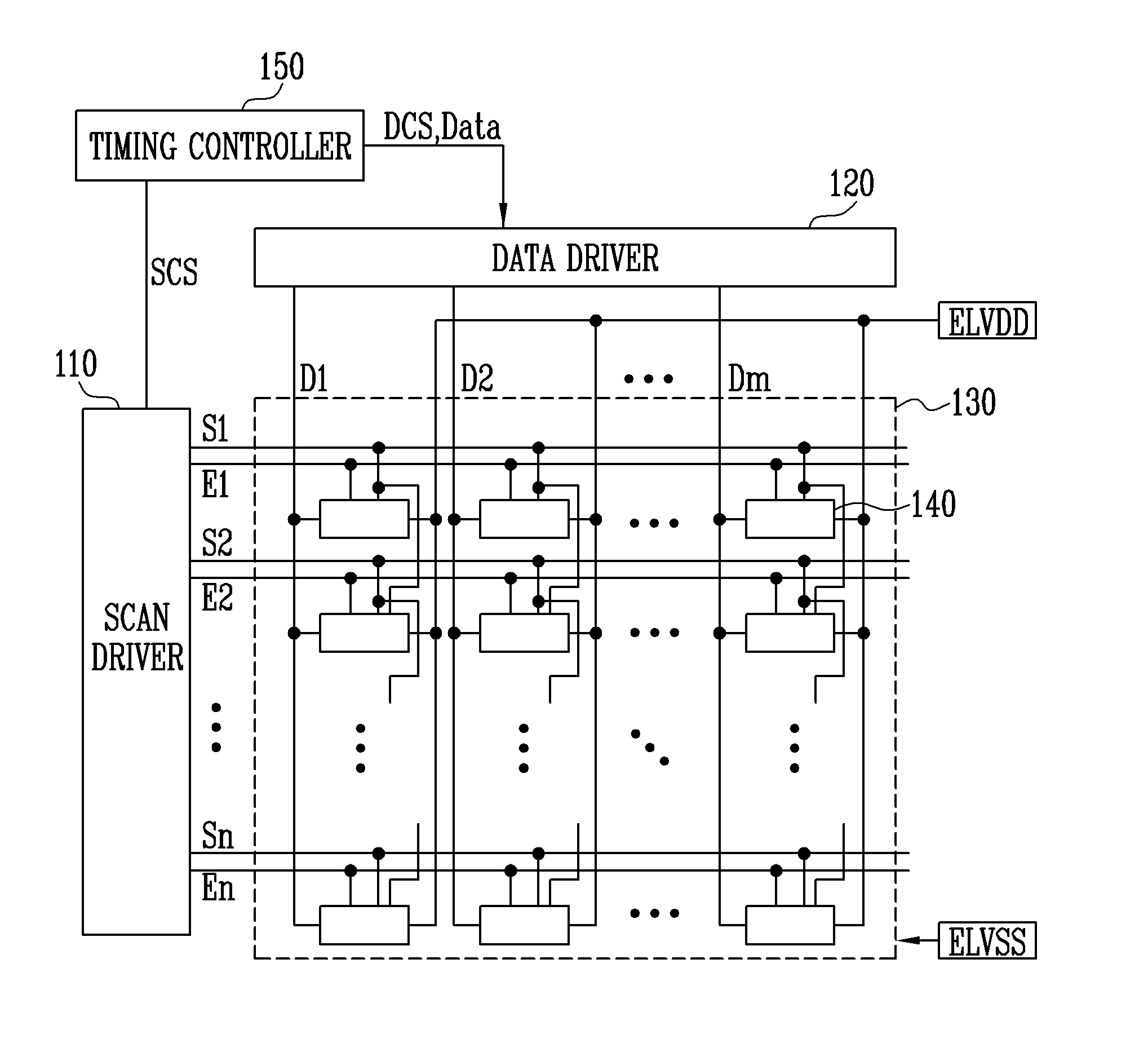
[0023]FIG. 1 is a block diagram illustrating an organic light emitting display device according to an embodiment of the present invention.

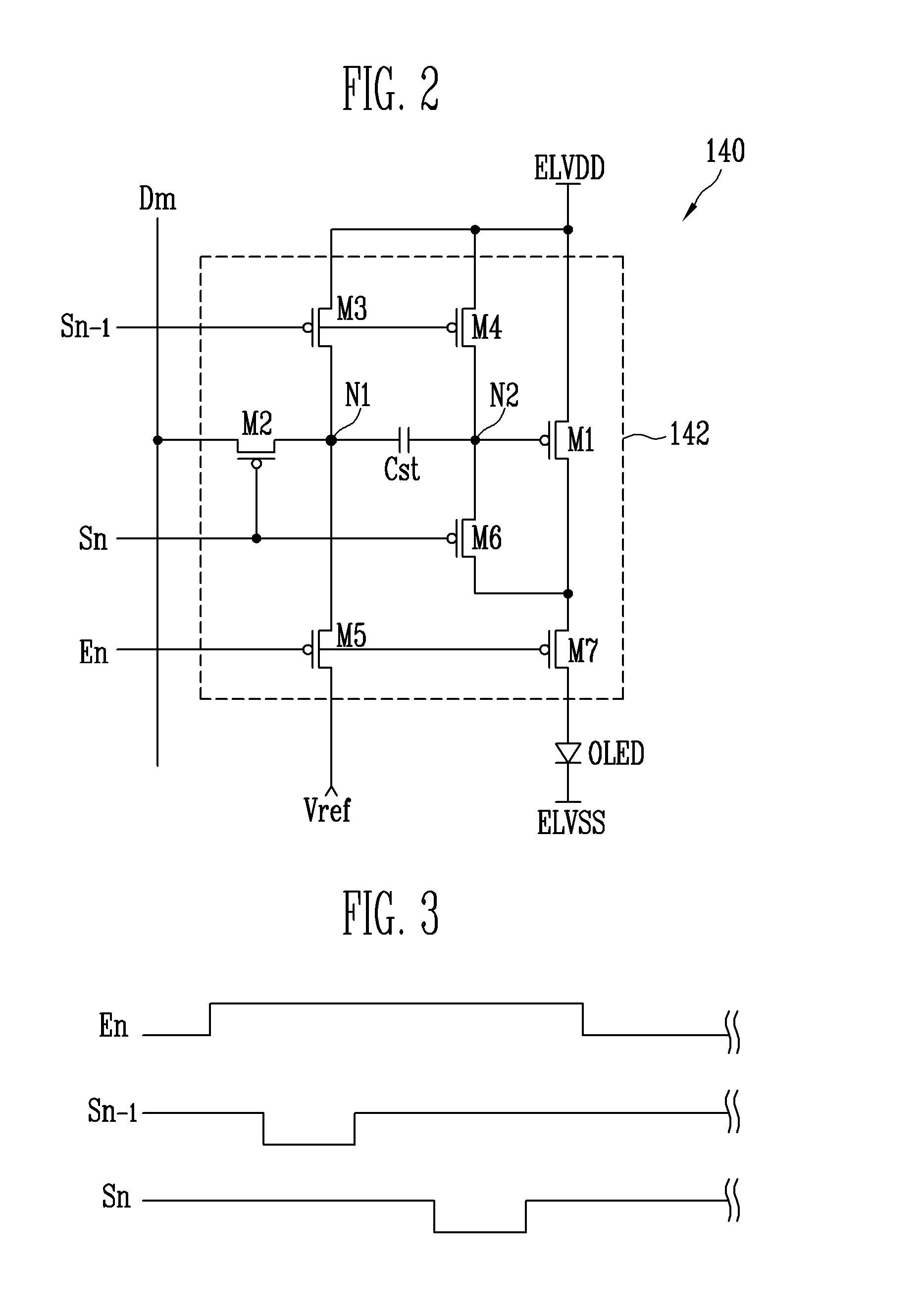
[0024]Referring to FIG. 1, the organic light emitting display device according to this embodiment includes a pixel unit 130 having pixels 140 positioned at intersection portions of scan lines S1 to Sn and data lines D1 to Dm, a scan driver 110 driving the scan lines S1 to Sn and emission contr...


PUM


Abstract

A structure of a pixel and an organic light emitting display device using the same are provided. The pixel includes an organic light emitting diode; a first transistor controlling the amount of current supplied from a first power source to the organic light emitting diode depending on a voltage applied to a second node; a second transistor coupled between a data line and a first node, and turned on when a scan signal is supplied to a first scan line; a third transistor coupled between the first power source and the first node, and turned on when the scan signal is supplied to a second scan line; a fourth transistor coupled between the first power source and the second node, and turned on when the scan signal is supplied to the second scan line; and a storage capacitor coupled between the first and second nodes.

Description

CLAIM OF PRIORITY[0001]This application claims priority to and the benefit of Korean Patent Application No. 10-2012-0145454, filed on Dec. 13, 2012, in the Korean Intellectual Property Office, the entire content of which is incorporated herein by reference.BACKGROUND[0002]1. Field of the Invention[0003]An aspect of the present invention relates to a pixel and an organic light emitting display device using the same, and more particularly, to a pixel and an organic light emitting display device using the same, which can improve image quality.[0004]2. Description of the Related Art[0005]Recently, various types of flat panel display devices capable of reducing the weight and volume of cathode ray tubes have been developed. The flat panel display devices include a liquid crystal display, a field emission display, a plasma display panel, an organic light emitting display device, and the like.[0006]Among these flat panel display devices, the organic light emitting display device displays i...

Claims


Application Information

Patent Timeline
Patent Type & Authority Applications(United States)
IPC IPC(8): G09G3/32H05B33/08H05B44/00
CPCG09G3/3233G09G2300/0842G09G2300/0861G09G2310/0262G09G2300/0819H05B45/60Y02B20/30G09G3/30
Inventor KIM, DONG-HWI
Owner SAMSUNG DISPLAY CO LTD
Why Eureka
Try Eureka