Fabrication of iii-v-on-insulator platforms for semiconductor devices

a technology of silicon-based platforms and silicon-based components, which is applied in the direction of semiconductor devices, electrical equipment, basic electric elements, etc., can solve problems such as defects in semiconductor devices

Inactive Publication Date: 2016-07-21
ELPIS TECH INC
View PDF0 Cites 0 Cited by
  • Summary
  • Abstract
  • Description
  • Claims
  • Application Information

AI Technical Summary

Problems solved by technology

III-V FETs on silicon platforms (e.g., such as CMOS platforms) can be difficult to fabricate on account of mismatched lattices of III-V materials and silicon, which can cause strain at the interfaces of such materials and result in defects in the semiconductor devices.

Method used


Image

  • Fabrication of iii-v-on-insulator platforms for semiconductor devices
  • Fabrication of iii-v-on-insulator platforms for semiconductor devices
  • Fabrication of iii-v-on-insulator platforms for semiconductor devices

Examples


Embodiment Construction

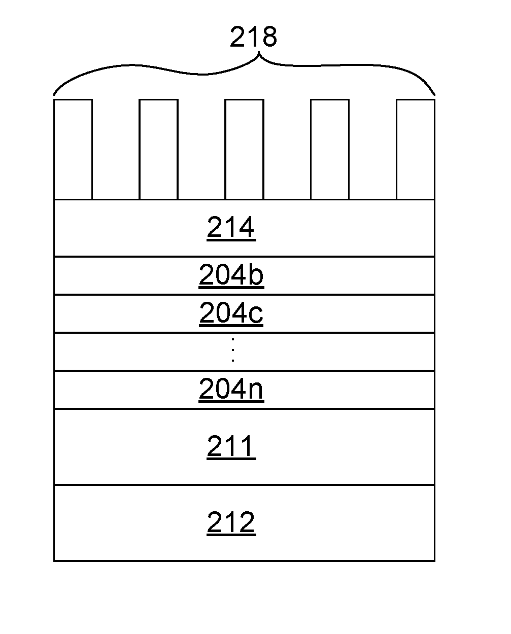
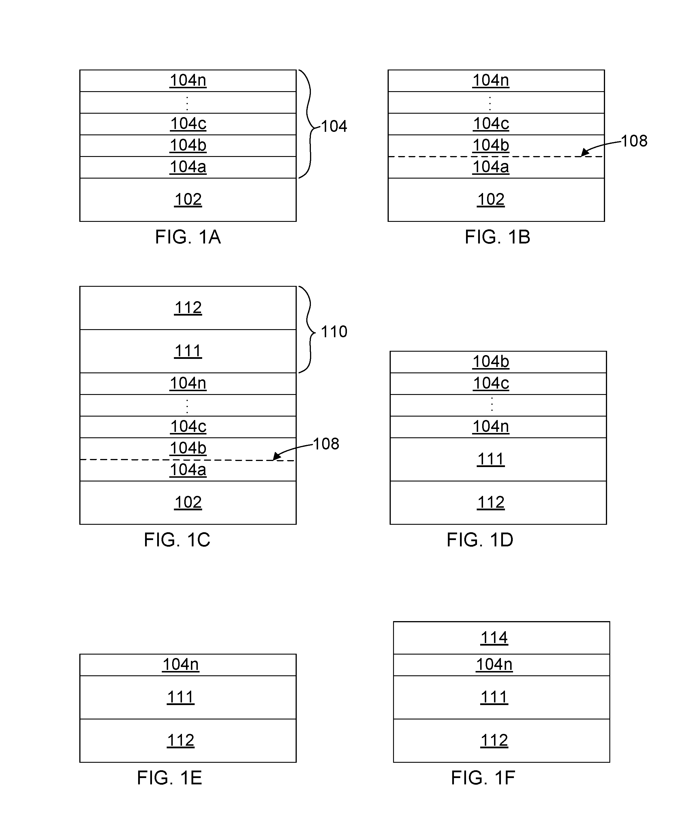
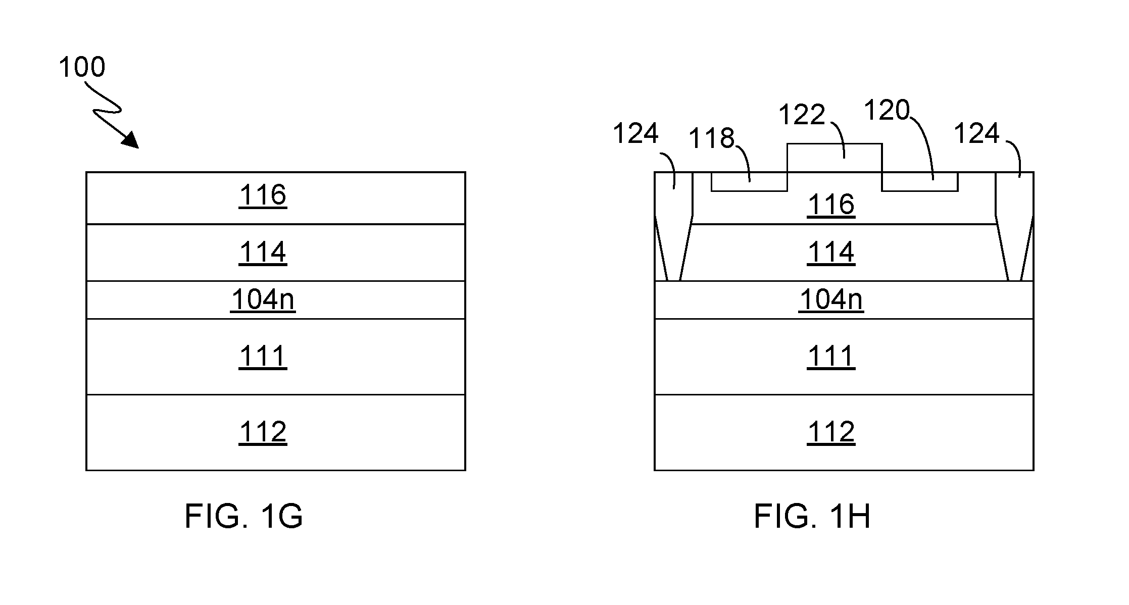
[0013]Embodiments of the present invention provide efficient, cost-effective IIIVOI platforms for semiconductor devices and methods for fabricating the same. In one embodiment, compositionally-graded buffer layers of III-V alloy are grown on a silicon substrate, and a smart cut technique is used to cut and transfer layers of III-V alloy to a handle substrate (e.g., a silicon wafer having an insulator layer, such as an oxide). One or more transferred layers of III-V alloy can be etched away to expose a desired transferred layer of III-V alloy, upon which a semi-insulating buffer layer and channel layer can be grown to yield a IIIVOI platform on which semiconductor devices (e.g., planar and / or 3-dimensional FETs) can be fabricated.

[0014]Detailed embodiments of the claimed structures and methods are disclosed herein; however, it is to be understood that the disclosed embodiments are merely illustrative of the claimed structures and methods that may be embodied in various forms. In addi...


PUM

PropertyMeasurementUnit
lattice constantaaaaaaaaaa

Abstract

Embodiments of the present invention provide III-V-on-insulator (IIIVOI) platforms for semiconductor devices and methods for fabricating the same. According to one embodiment, compositionally-graded buffer layers of III-V alloy are grown on a silicon substrate, and a smart cut technique is used to cut and transfer one or more layers of III-V alloy to a silicon wafer having an insulator layer such as an oxide. One or more transferred layers of III-V alloy can be etched away to expose a desired transferred layer of III-V alloy, upon which a semi-insulating buffer layer and channel layer can be grown to yield IIIVOI platform on which semiconductor devices (e.g., planar and / or 3-dimensional FETs) can be fabricated.

Description

FIELD OF THE INVENTION[0001]The present invention relates generally to the field of semiconductor devices, and more particularly to III-V-on-insulator (IIIVOI) platforms for semiconductor devices.BACKGROUND OF THE INVENTION[0002]The fabrication of semiconductor devices involves forming electronic components in and on semiconductor substrates, such as silicon wafers. These electronic components may include one or more conductive layers, one or more insulation layers, and doped regions formed by implanting various dopants into portions of a semiconductor substrate to achieve specific electrical properties.[0003]Field-effect transistors (FETs), such as planar metal-oxide-semiconductor FETs (MOSFETs) and 3-dimensional FinFETs, are semiconductor devices. Silicon on insulator (SOI) platforms for FETs comprise layered silicon-insulator-silicon substrates on which FETs can be built, and such platforms can reduce parasitic device capacitance and improve performance.[0004]III-V FET technologi...

Claims


Application Information

Patent Timeline
Patent Type & Authority Applications(United States)
IPC IPC(8): H01L21/762H01L21/265H01L29/66H01L21/02
CPCH01L21/76254H01L21/02463H01L21/0251H01L29/66522H01L21/02381H01L21/02546H01L29/66795H01L21/2654H01L21/7605H01L29/20H01L29/785H01L29/78603H01L29/78681H01L21/02505H01L29/0649
Inventor BASU, ANIRBANHEKMATSHOARTABARI, BAHMANKHAKIFIROOZ, ALISHAHRJERDI, DAVOOD
Owner ELPIS TECH INC
Why Eureka
Try Eureka