Method for fabricating sensing device

Inactive Publication Date: 2016-07-21
PRIMAX ELECTRONICS LTD
View PDF10 Cites 3 Cited by
  • Summary
  • Abstract
  • Description
  • Claims
  • Application Information

AI Technical Summary

Benefits of technology

[0007]An object of the present invention provides a method for

Problems solved by technology

In other words, the method of fabricating the conventi

Method used


Image

  • Method for fabricating sensing device
  • Method for fabricating sensing device
  • Method for fabricating sensing device

Examples


Example

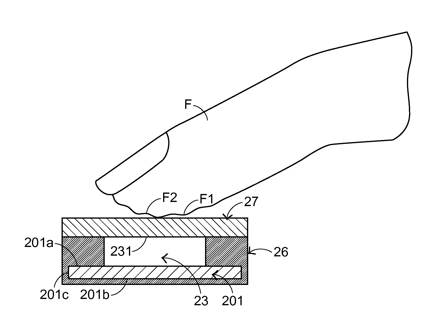
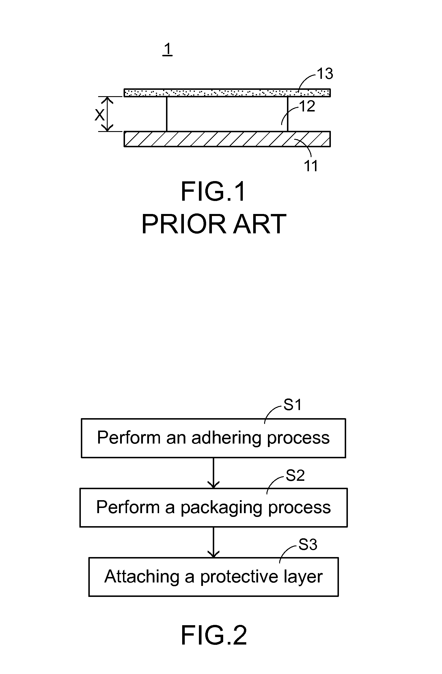
[0021]The present invention provides a method for fabricating a sensing device. As shown in FIG. 2, the fabricating method comprises the following steps. In a step S1, an adhering process is performed. In a step S2, a packaging process is performed. In a step S3, a protective layer is attached on a sensing surface. These steps will be illustrated in more details as follows.

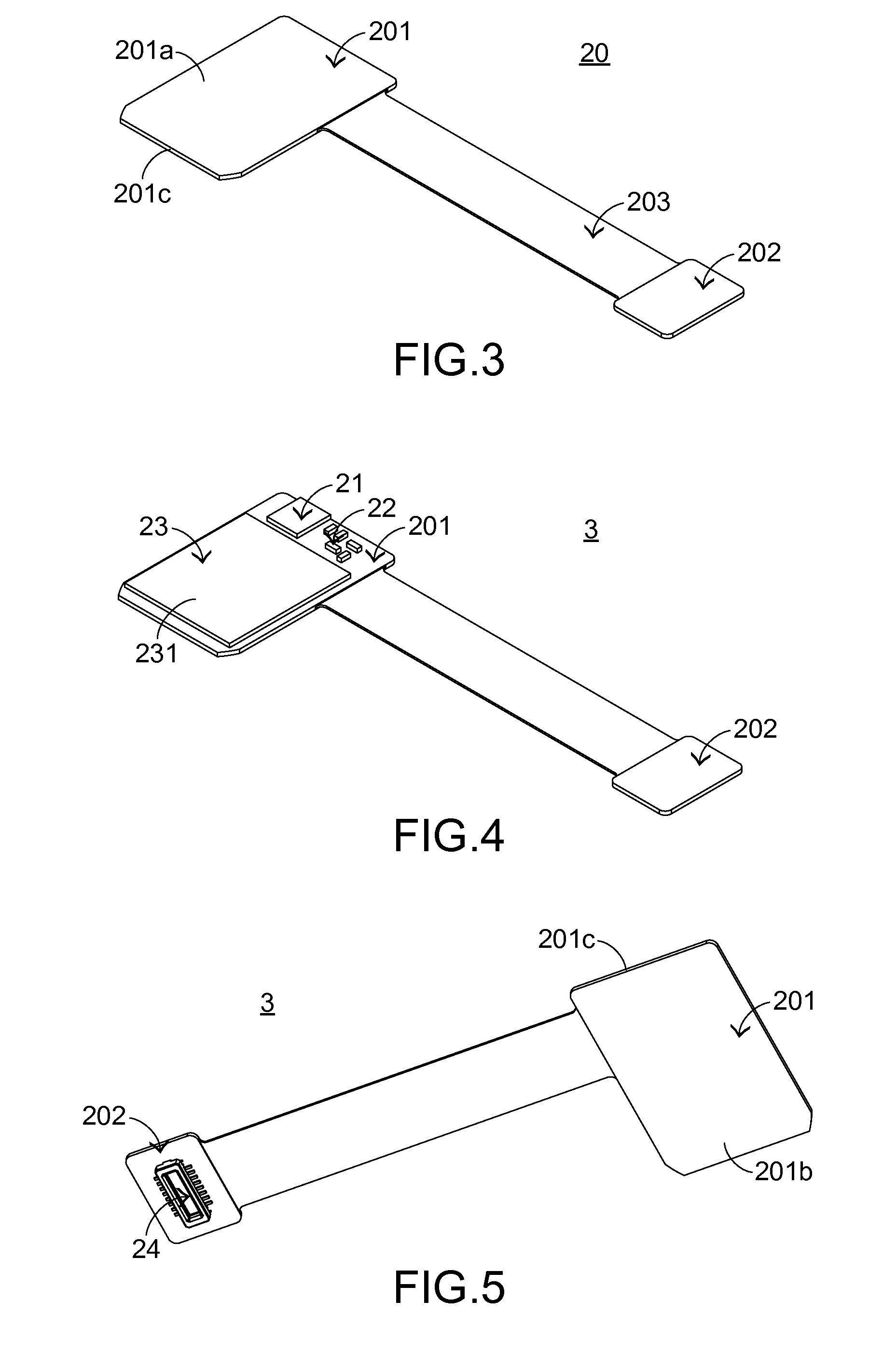
[0022]FIG. 3 is a perspective view illustrating a circuit board assembly of a sensing device according to an embodiment of the present invention. The circuit board assembly 20 is provided for performing the subsequent steps (i.e. the adhering process S1, the packaging process S2 and the protective layer attaching process S3). In this embodiment, the circuit board assembly 20 is a rigid-flex board assembly. The circuit board assembly 20 comprises a first circuit board 201, a second circuit board 202 and a flexible printed circuit board (FPCB) 203. The first circuit board 201 and the second circuit board 202 are rig...


PUM


Abstract

A method for fabricating a sensing device includes the following steps. Firstly, an adhering process is performed to attach a sensing integrated circuit on a first circuit board, wherein the sensing integrated circuit has a sensing surface. Then, a packaging process is performed to encapsulate the first circuit board within a package shell, so that at least a portion of a top surface of the first circuit board is covered by the package shell. The sensing surface of the sensing integrated circuit is exposed to a top surface of the package shell. Afterwards, a protective layer is attached on the sensing surface.

Description

FIELD OF THE INVENTION[0001]The present invention relates to a method for fabricating a sensing device, and more particularly to a method for fabricating a fingerprint sensing device.BACKGROUND OF THE INVENTION[0002]Nowadays, a fingerprint sensing device is gradually applied to a portable electronic device. The principles of the fingerprint sensing device will be described as follows. A sensing electrode layer is integrated into a chip. When a surface of the chip is pressed by a user's finger, the ridges and the valleys of a user's finger generate different capacitance values on the sensing electrode layer, and the fingerprint image of the user's finger is acquired by the chip according to the capacitance values.[0003]The structure of a conventional fingerprint sensing device 1 is shown in FIG. 1. The method of fabricating the conventional fingerprint sensing device 1 will be illustrated as follows. Firstly, a circuit board 11 is provided. Then, a sensing chip 12 is installed on a t...

Claims


Application Information

Patent Timeline
IPC IPC(8): H05K3/28H05K3/36G06K9/00H05K3/30
CPCH05K3/284G06K9/0002H05K3/361H05K3/305G06V40/1329
Inventor CHENG, CHIA-CHUCHU, CHIH-CHUANG
Owner PRIMAX ELECTRONICS LTD
Why Eureka
Try Eureka