Opto-electric hybrid board, and production method therefor
a hybrid board and opto-electric technology, applied in the direction of conductive pattern formation, printed circuit non-printed electric components association, instruments, etc., can solve the problems of liable light transmission loss of the flexible optical waveguide w other than the boundary, liable to break or fold at the boundary, etc., to achieve easy provision of inventive opto-electric hybrid boards, reduce the light transmission loss of the resulting optical waveguide, and avoid unnecessary steps
- Summary
- Abstract
- Description
- Claims
- Application Information
AI Technical Summary
Benefits of technology
Problems solved by technology
Method used
Image
Examples
example 1
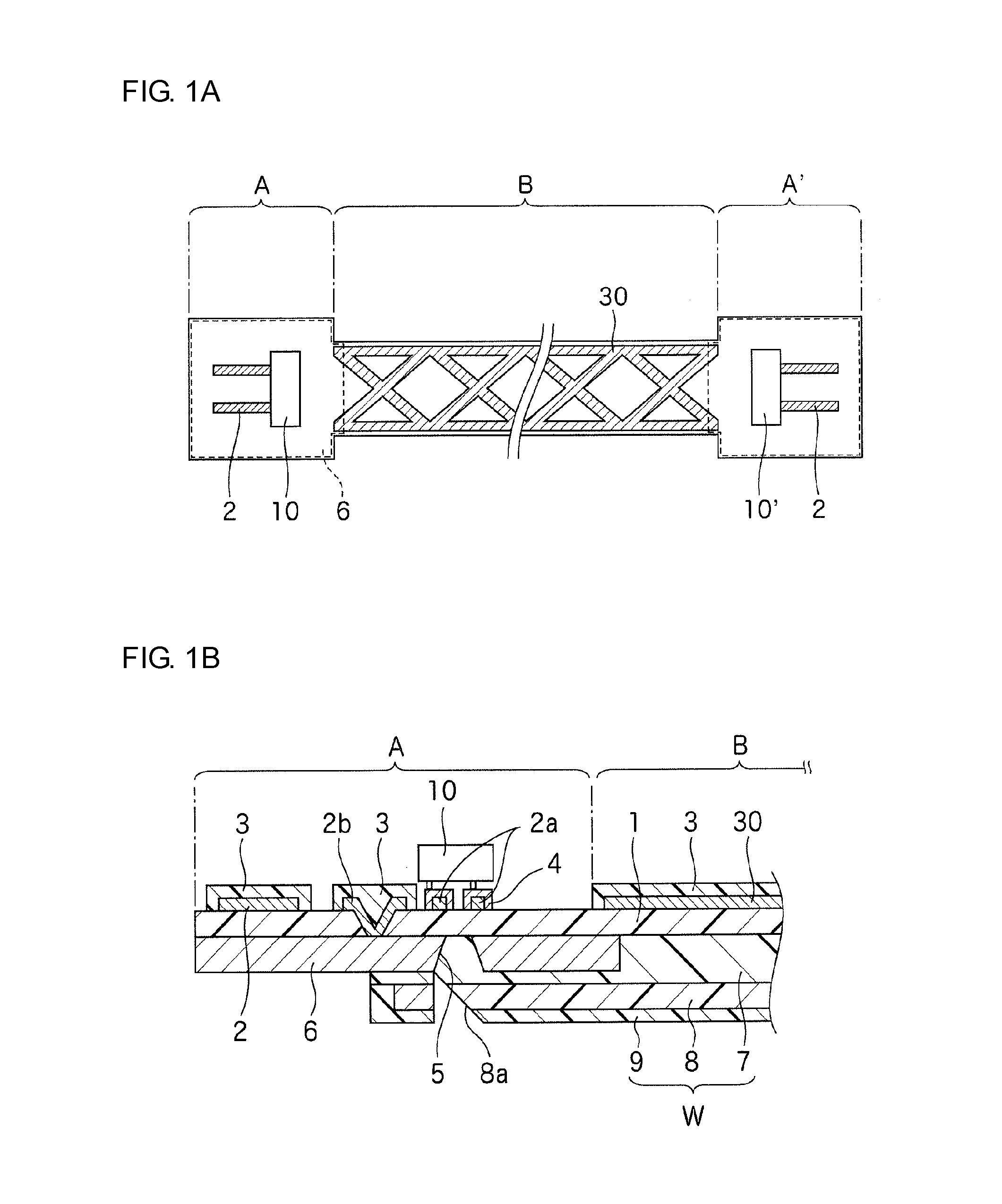
[0068]The opto-electric hybrid board shown in FIGS. 1A and 1B was produced in the aforementioned manner. The interconnection portion B had a length of 20 cm. A 20-μm thick stainless steel layer was provided as the metal reinforcement layer. The insulation layer had a thickness of 5 μm, and the under-cladding layer had a thickness of 10 μm (as measured from the back surface of the insulation layer). The core had a thickness of 50 μm and a width of 50 μm. The over-cladding layer had a thickness of 70 μm (as measured from the front surface of the under-cladding layer). The first electric wiring and the electrically conductive dummy pattern had a thickness of 5 μm. The electrically conductive dummy pattern had an oblique lattice shape, and covered the insulation layer at a surface coverage percentage of 44%. The electrically conductive dummy pattern had edge portions respectively extending continuously along the opposite longitudinal edges of the interconnection portion and each having ...
example 2
[0069]An opto-electric hybrid board having substantially the same basic construction as in Example 1, except that electrically conductive dummy patterns were formed in an arrangement as shown in FIG. 7 and no second electric wiring was formed. The electrically conductive dummy patterns covered the surface of the insulation layer at a surface coverage percentage of 40%. Longitudinal edge portions of the electrically conductive dummy patterns respectively extending continuously along the opposite longitudinal edges of the insulation layer each had a width (indicated by a reference character Q′ in FIG. 7) of 400 μm.
PUM
 Abstract
Description
Claims
Application Information
 - R&D
- Intellectual Property
- Life Sciences
- Materials
- Tech Scout
- Unparalleled Data Quality
- Higher Quality Content
- 60% Fewer Hallucinations
Browse by: Latest US Patents, China's latest patents, Technical Efficacy Thesaurus, Application Domain, Technology Topic, Popular Technical Reports.
© 2025 PatSnap. All rights reserved.Legal|Privacy policy|Modern Slavery Act Transparency Statement|Sitemap|About US| Contact US: help@patsnap.com


