Packaged Microchip with Patterned Interposer

Inactive Publication Date: 2016-08-11
ANALOG DEVICES INC
View PDF10 Cites 5 Cited by
  • Summary
  • Abstract
  • Description
  • Claims
  • Application Information

AI Technical Summary

Benefits of technology

This patent text describes a packaged microchip with an interposer between the base and the die that helps to reduce stress and mitigate the effects of thermal expansion. The interposer has a recess on its first side with a top area that is smaller than the die area, which can be connected to both the die and the base. The top area of the interposer is also less than half of its die area. The method of forming the packaged microchip involves coupling the interposer to the die using adhesive, whether it is positioned within the recess or a thin adhesive film is used.

Problems solved by technology

Problems can arise, however, when the temperatures of the two surfaces change.
Substrate bending or flexing consequently can affect movement of the die structures and the functioning of the electronics, thus causing the output data representing the property being measured (e.g., acceleration) to be erroneous.
In a similar manner, mechanically induced linear or torsional stress applied to the package also can be translated to the die, thus causing the same undesirable effects.

Method used


Image

  • Packaged Microchip with Patterned Interposer
  • Packaged Microchip with Patterned Interposer
  • Packaged Microchip with Patterned Interposer

Examples


Embodiment Construction

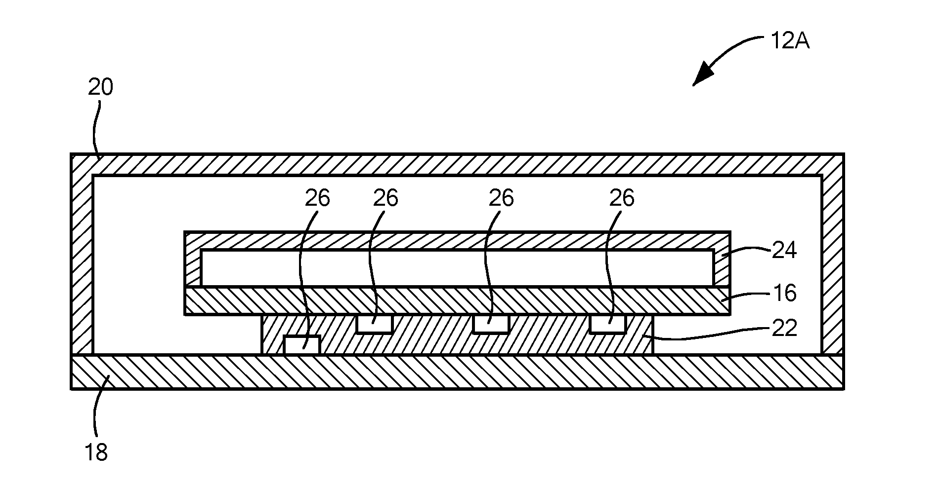
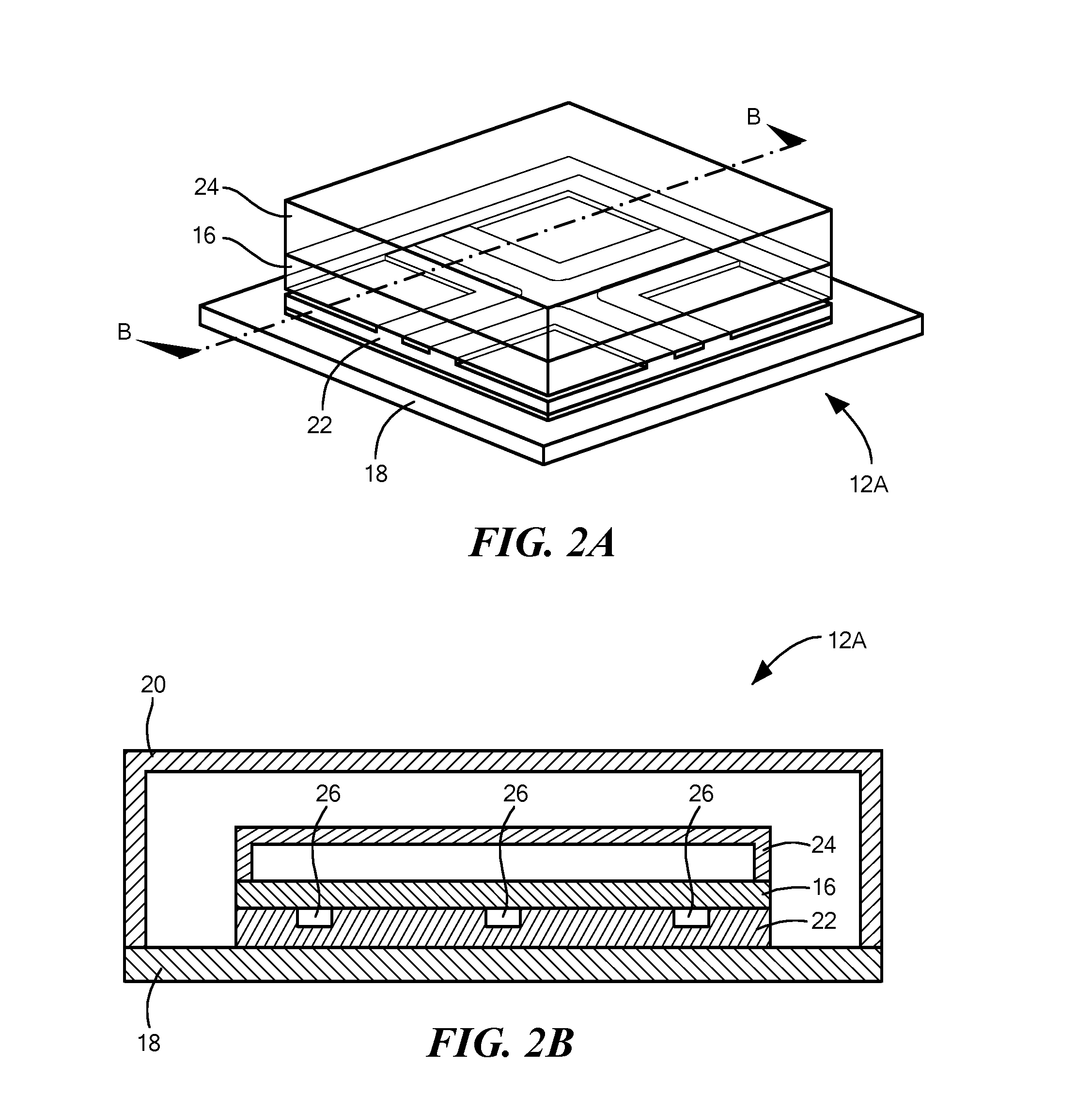
[0007]In accordance with one embodiment of the invention, a packaged microchip has a base, a die with a mounting surface, and an electrically inactive interposer between the base and the die. The interposer has a first side with at least one recess that extends no more than part-way through the interposer from the first side. Accordingly, the recess defines a top portion (of the first side) with a top area. The die mounting surface, which is coupled with the interposer, correspondingly has a die area. The top area of the interposer preferably is less than the die area.

[0008]The top surface of the interposer can be mounted to either the die or the base. To that end, the mounting surface of the die may couple with the first side of the interposer. Alternatively, the first side of the interposer may couple with the base. Moreover, adhesive may couple the interposer to the base and / or the die. For example, adhesive may be within the at least one recess to connect the interposer to the b...


PUM

PropertyMeasurementUnit
Adhesivityaaaaaaaaaa
Microstructureaaaaaaaaaa
Areaaaaaaaaaaa

Abstract

A packaged microchip has a base, a die with a mounting surface, and an electrically inactive interposer between the base and the die. The interposer has a first side with at least one recess that extends no more than part-way through the interposer from the first side. Accordingly, the recess defines a top portion (of the first side) with a top area. The die mounting surface, which is coupled with the interposer, correspondingly has a die area. The top area of the interposer preferably is less than the die area.

Description

PRIORITY[0001]This patent application claims priority from Provisional U.S. Patent Application No. 62 / 114,741, filed Feb. 11, 2015, entitled, “MEMS DEVICE WITH PATTERNED INTERPOSER,” and naming Bradley C. Kaanta, John A. Alberghini, and Kemiao Jia as inventors, the disclosure of which is incorporated herein, in its entirety, by reference.FIELD OF THE INVENTION[0002]The disclosure generally relates to microchips and, more particularly, the disclosure relates to packaging techniques for microchips.BACKGROUND OF THE INVENTION[0003]Microelectromechanical systems (“MEMS”) are used in a growing number of applications. For example, MEMS currently are implemented as gyroscopes to detect pitch angles of airplanes, and as accelerometers to selectively deploy air bags in automobiles. In simplified terms, such MEMS devices typically have a structure suspended above a substrate, and associated electronics that both senses movement of the suspended structure and delivers the sensed movement data ...

Claims


Application Information

Patent Timeline
IPC IPC(8): B81B7/00B81C1/00
CPCB81C1/00269B81B7/0048
Inventor KAANTA, BRADLEY C.ALBERGHINI, JOHN A.JIA, KEMIAO
Owner ANALOG DEVICES INC
Why Eureka
Try Eureka