
Liquid crystal display panel

a liquid crystal display and panel technology, applied in static indicating devices, non-linear optics, instruments, etc., can solve the problems of delay distortion, serious color shift problems, and non-uniform color display in images containing multiple colors, and achieve the effect of reducing the color shift phenomenon

Active Publication Date: 2016-08-25
TCL CHINA STAR OPTOELECTRONICS TECH CO LTD
View PDF3 Cites 9 Cited by
  • Summary
  • Abstract
  • Description
  • Claims
  • Application Information

AI Technical Summary

Benefits of technology

The present disclosure provides a liquid crystal display panel and a method for manufacturing it that can alleviate the color shift phenomenon. This is achieved by arranging data lines with different widths that change gradually in the active area to substitute traditional data lines with the same width. This reduces the impedance difference between data lines in different parts of the panel, such as the right side and left side, and the central part. This helps to improve the color accuracy and consistency of the liquid crystal display panel.

Problems solved by technology

During design and production of liquid crystal display panel, how to avoid the color shift phenomenon is an important challenge faced by the Research & Development personnel.
The color shift phenomenon means that the colors displayed in an image containing multiple colors are non-uniform when the image is presented, and the image would contain more ingredients of a certain color.
For instance, the poor quality of the video signal lines (data lines) or the poor contact thereof would result in serious color shift problems.
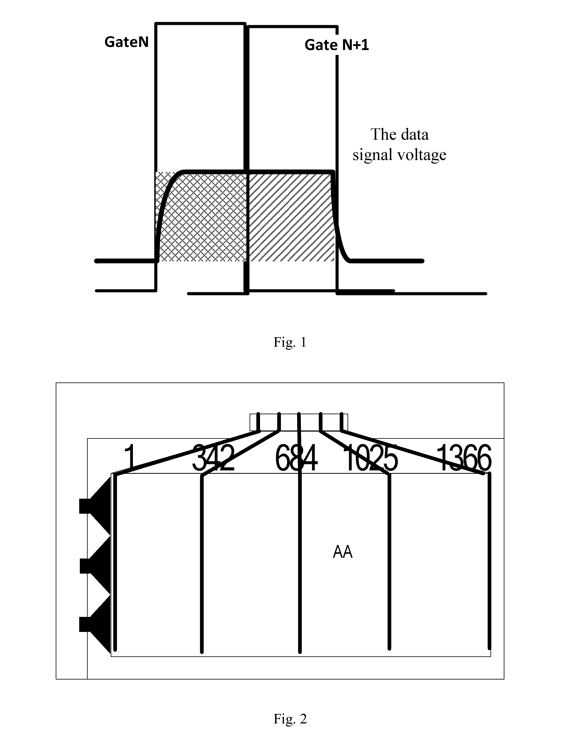
Since the data wirings have a certain impedance, which is equivalent to an RC network in series connection, a certain delay distortion must occur to the data signal voltage during transmission, and thus the electric potential of the pixel electrode of the pixel unit cannot completely reach an electric potential of the data signal voltage output by the data driving module.

Method used


Image

  • Liquid crystal display panel
  • Liquid crystal display panel
  • Liquid crystal display panel

Examples


embodiment 1

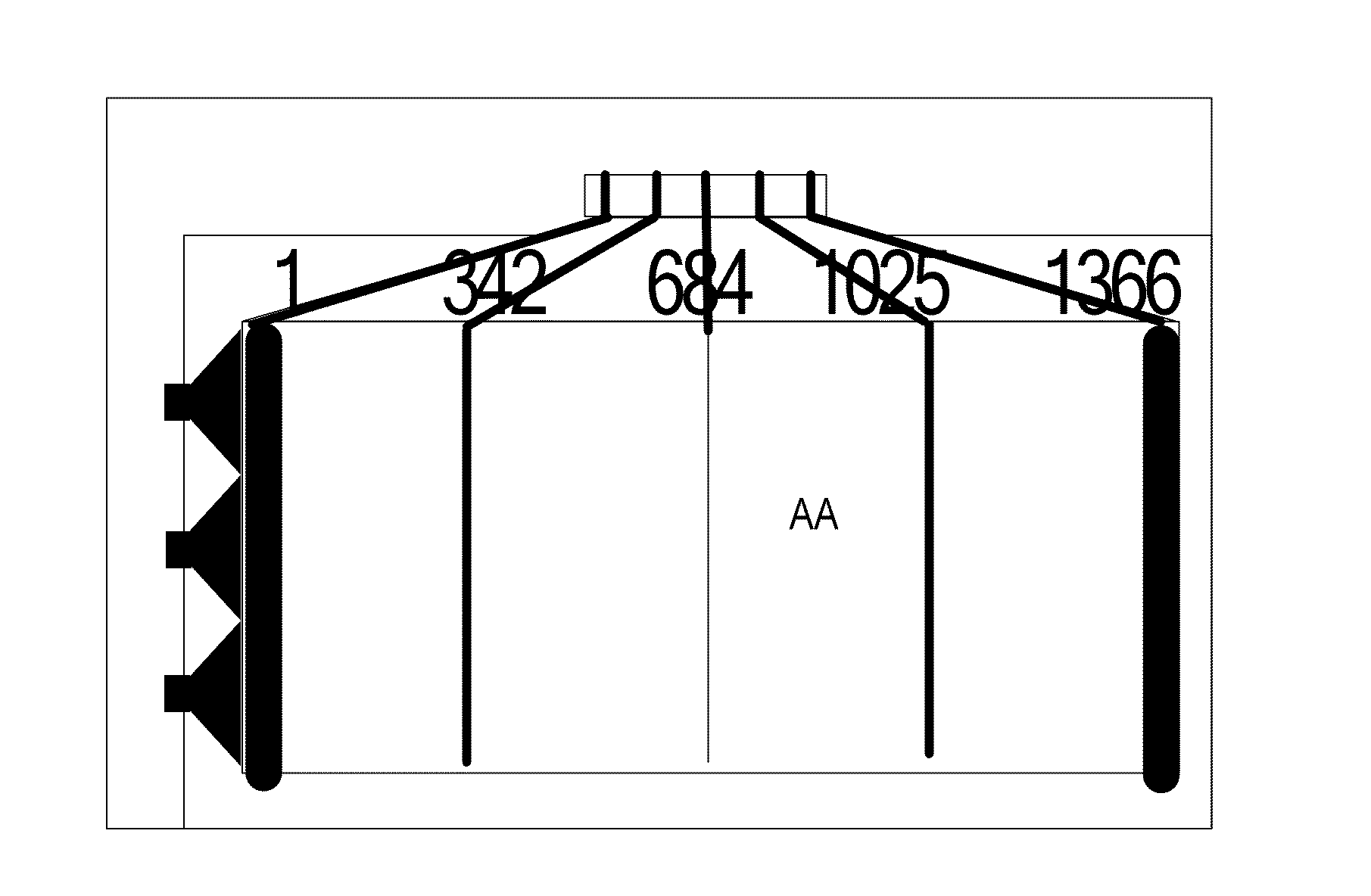
[0035]FIG. 3 shows a specific embodiment of the present disclosure. According to the present disclosure, the widths of the data lines in the active area increase gradually from a central part of the active area to a right side and a left side thereof. This arrangement is mainly applicable to the situation that the value of Rfanout of each data line in the fanout area is far less than the value of Cfanout thereof. Under this circumstance, the resistance values Rdata of the data lines would decrease with the increasing of the widths of the data lines in the active area, and accordingly, the capacitance values Cdata of the data lines in the active area would increase. However, since the capacitance value Cfanout of each data line in the fanout area is relatively large, the changing of (Cfanout+Cdata) is relatively small, and thus its influence on the time-delay constant RCdelay is small as well. From the whole point of view, the time-delay constants RCdelay of the data lines in the rig...

embodiment 2

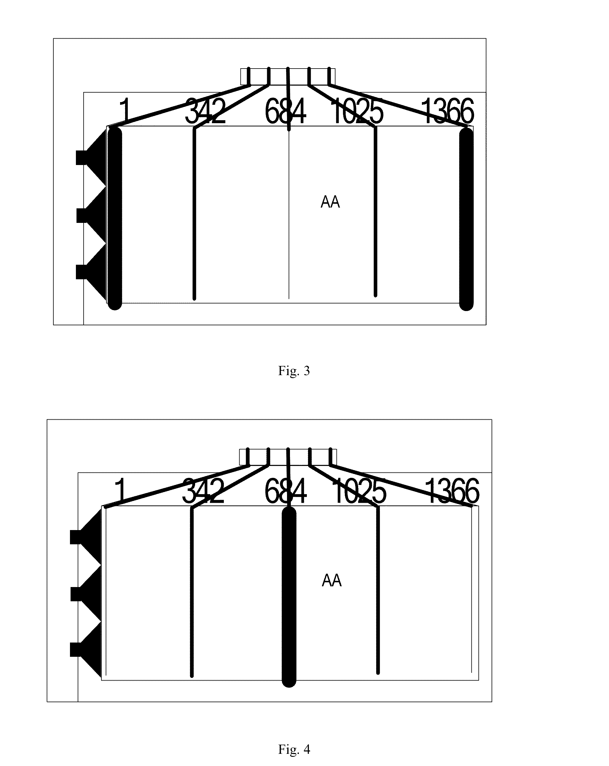
[0037]FIG. 4 shows another specific embodiment of the present disclosure. According to the present disclosure, the widths of the data lines in the active area decrease gradually from a central part of the active area to a right side and a left side thereof. This arrangement is mainly applicable to the situation that the value of Rfanout of each data line in the fanout area is far more than the value of Cfanout thereof. Under this circumstance, the capacitance values Cdata of the data lines would decrease with the decreasing of the widths of the data lines in the active area, and accordingly, the resistance values Rdata of the data lines in the active area would increase. However, since the resistance value Rfanout of each data line in the fanout area is relatively large, the changing of (Rfanout+Rdata) is relatively small, and thus its influence on the time-delay constant RCdelay is small as well. From the whole point of view, the time-delay constants RCdelay of the data lines in th...

embodiment 3

[0039]FIG. 5 shows a third specific embodiment of the present disclosure. According to the present embodiment, the width of each of the data lines arranged in a right side and a left side of the active area decreases uniformly along a direction from an upper end of the active area to a lower end of the active area, while the width of each of the data lines arranged in a central part of the active area increases uniformly along the direction from the upper end of the active area to the lower end of the active area. In this case, although the width of each of the data lines arranged in the right side and the left side of the active area decreases uniformly along the direction from the upper end of the active area to the lower end thereof, for the whole data line, the capacitance value Cdata is almost unchanged, while the growth of the resistance value Rdata decreases gradually with the increasing of the length of the data line. Similarly, although the width of each of the data lines a...


PUM

PropertyMeasurementUnit
widthsaaaaaaaaaa
widthaaaaaaaaaa
areaaaaaaaaaaa

Abstract

A liquid crystal display panel and a method for manufacturing the same are disclosed. The liquid crystal display panel comprises a data driving module; data lines arranged in an active area in parallel with one another; and data wirings arranged in a fanout area, one end of each data wiring being connected with an output end of said data driving module, the other end thereof being connected with a data line of said active area, wherein the data lines in said active area are arranged to have different widths.

Description

CROSS REFERENCE TO RELATED APPLICATION[0001]The present application claims benefit of Chinese patent application CN 201410799546.8, entitled “Liquid Crystal Display Panel” and filed on Dec. 19, 2014, which is incorporated herein by reference.FIELD OF THE INVENTION[0002]The present disclosure relates to the technical field of liquid crystal display, and particularly to a liquid crystal display panel that can alleviate the color shift phenomenon, and a manufacturing method thereof.BACKGROUND OF THE INVENTION[0003]The liquid crystal display device, especially the Thin Film Transistor Liquid Crystal Display (TFT-LCD) has been widely used in computers, flat televisions, mobile phones and other information products due to its outstanding performance. During design and production of liquid crystal display panel, how to avoid the color shift phenomenon is an important challenge faced by the Research & Development personnel. The color shift phenomenon means that the colors displayed in an im...

Claims


Application Information

Patent Timeline
Patent Type & Authority Applications(United States)
IPC IPC(8): G02F1/1362
CPCG02F1/136286G02F1/1362G02F2201/18G09G2300/0426G09G2320/0223G09G2320/0242G02F1/136295
Inventor LIAO, ZUOMINHAN, BING
Owner TCL CHINA STAR OPTOELECTRONICS TECH CO LTD
Learn More